Products
FIB-SEM
Nanomanipulators
OmniProbeOmniProbe CryoSoftware
AZtec3DAZtecFeatureAZtec LayerProbeTEM
Hardware
EDSUltim MaxXploreImaging
TEM CamerasSoftware
AZtecTEM
 Part of the Oxford Instruments Group
10th November 2021 | Author: Dr Lucia Spasevski
Semiconductors have revolutionised the way we live today. They are everywhere around us - in smartphones, digital cameras, televisions, washing machines, CPUs, refrigerators, LED bulbs and more, and they help us to live more comfortable lives. The ubiquitous little black "chips" you find on just about every circuit board, the integrated circuits (ICs), are the fundamental building block of all modern electronic devices. They contain millions or billions of transistors, resistors, capacitors & logic gates, all connected on a thin substrate of semiconductor material (usually silicon crystal) to form a complex digital circuit.
Making these tiny devices is an enormous engineering challenge, but a surprising problem faced by IC manufacturers is the ability to inspect them. With semiconductor device scaling, performance and reliability is even more sensitive to local chemistry, size and shape of device circuitry. In order to increase manufacturing yield, rapid detection and analysis of defects is also a prerequisite. AZtecLive can be employed at any step of the IC manufacturing process, and it is a great help in quick examination of different circuit structures, thanks to its Live Chemical Imaging capability. Using AZtecLive, regions of interest can be quickly located and examined in more detail when appropriate.
In this blog post we show how Live Chemical Imaging can be used to examine a prior-generation silicon chip containing multiple integrated circuits on the mm to µm scale.
In traditional EDS mapping, it is not possible to get chemical information before choosing a site of interest on a sample, but with the introduction of Live Chemical Imaging, that limitation has been overcome. We can now easily investigate the sample by simultaneously acquiring EDS data and electron images while moving the stage. This post will serve as an introduction to the use of live chemical imaging on a semiconductor sample, but if you would like to learn more, please join us for our upcoming webinar "Revolutionise your SEM capabilities with Live Chemical Imaging".
We start the inspection of the sample by selecting Live Chemical Imaging navigator step in AZtecLive. While moving around the sample, we can see a vast array of lines stretching across the wafer. These are aluminium microscale wires that serve as a global highway of information and power flowing across the chip. It is easy to spot different parts of circuitry and even to collect the signal from phosphorous doping. Regions of the chip are treated (doped) with impurities that change the electrical properties of the silicon and our Ultim Max EDS detector is capable of delivering remarkable performance mapping signals from these dopants.
Immediately, we can spot some contamination by tracking the pink X-ray map corresponding to carbon. Contamination is a significant problem threatening the reliability of chips. In semiconductor manufacturing, even extremely small defects (protrusions, pattern deformation, scratches etc.) and foreign particles can cause performance issues. In this example, contamination is composed of organic matter (C and O) and some salts (major elements: K and CI), including Ca.
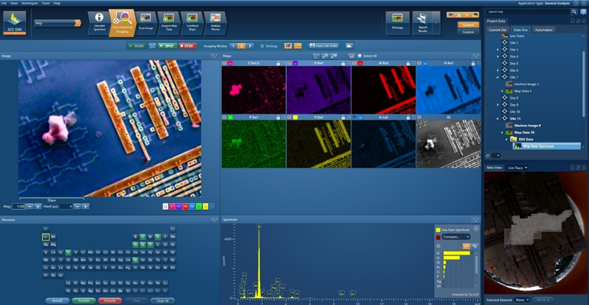
Figure 1. Contamination particle easily spotted using AztecLive
Now, let’s have a closer look of the wire structure on the left and explore what type of information we can extract from that part of the chip.
A quick glance in the EDS mapping pane of Live Chemical Imaging reveals that the silicon EDS signal is originating from the chip wafer. It’s clear for the user to see how the oxygen map overlaps with silicon due to the top silicon dioxide layer of the chip which serves as an insulation layer. All interconnects are easily resolved in the aluminium map, and it is possible to conclude that titanium is located underneath the aluminium layer. It’s also clear that certain parts of the circuity are missing their Al coating. A thin layer of Ti is often deposited to help other metals to stick to surfaces, or it can serve as a protective layer to stop Al diffusion into Si layer, even though nowadays it is not that commonly used.
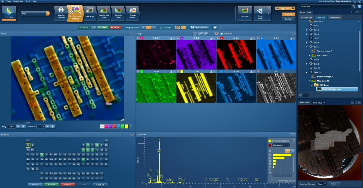
Figure 2. Examination of circuitry shape and chemistry
If we have a look at the structures appearing to the right of the wires, it is evident how the underlying layers influence those above and that the surface is wavy due to the continuous deposition of layers on top of each other leading to surface roughness. In more modern chips, layers are polished periodically throughout the fabrication process, so this effect is less prominent.
In the bottom right corner of Figures 1 and 2 you can see a Live Trace Mini View with a registered image. The registered image can be a schematic of the device or simply a photograph, and once registered, this image is automatically displayed as a background image that can be used to help navigate around the sample. Rectangles represent the size and position of each scanned field on the specimen. The current field of view is highlighted in blue. Within mini view, the user can select certain element to be displayed. All fields containing the element are shown in red. For example, we can select C and then, in the mini view, easily distinguish between scanned fields that contain organic contamination. The brighter the shade of red, the greater the weight % of the element in that field. It is even possible to select a field from the main workspace (highlighted in yellow) and then click "Move To" to move the microscope stage to selected field of view.
Another useful feature of AZtecLive is that, while navigating around the sample, the user can choose to track elements of interest in the overlay image. For example, it is possible to only select the Al signal to be overlaid on the electron image and to focus on any interruption in Al coating or to select to view only the C map to specifically for organic contamination.
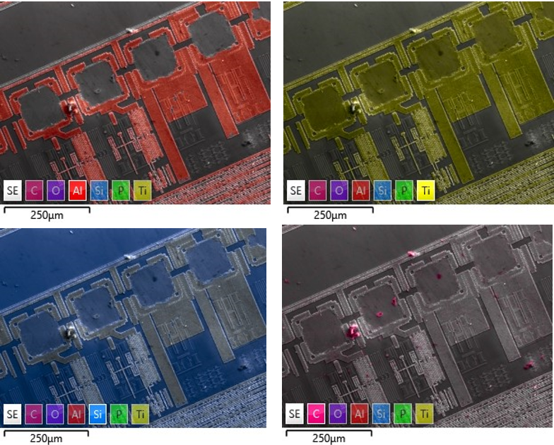
Figure 3. Selection of different elements of interest while navigating around sample
In the video below, you can see what type of information can be extracted from IC sample when observed using Live Chemical Imaging in Aztec 6.0.
We hope this blog has highlighted how AZtecLive can be helpful for easy navigation and investigation of large surface area electronic components. It has shown how users can quickly spot surface contaminants or failure structures and, at the same time, obtain important chemical information about them.
To learn more about our AZtecLive, click here and don’t forget to watch our upcoming webinar "Revolutionise your SEM capabilities with Live Chemical Imaging".
We send out monthly newsletters keeping you up to date with our latest developments such as webinars, new application notes and product updates.
© Oxford Instruments 2024