One of the common questions that I’m asked during my webinars is about tips and tricks for biological SEM electron imaging and collecting energy dispersive x-ray spectrometry (EDS) maps.
Here is a handy list to help you get the best out of your microscope.
Reduce or eliminate charging
Charging is a big issue with biological SEM and other non-conductive samples. It can also affect your EDS results and should be eliminated from your samples if at all possible. There are several strategies you can use.
Optimise your SEM sample preparation to make your sample as conductive as possible
- Thin sections of tissue/sample are less prone to charging. Make use of resin embedded samples on grids and using STEM holders for SEM or put sections directly onto a conductive substrate such as an aluminium stub or silicon wafer.
- Trim bulk samples to the smallest volume possible for your application. If you are looking at tissue, organs or parts of an organism try dissecting the sample to remove some of the bulk and optimise your images.
- Use heavy metal stains to improve conductivity and visualisation of your sample.
- Coat the sample with conductive materials (for example, carbon, gold, platinum/palladium). Some coating may affect your EDS results so make sure that you select the correct one for your application.
- Make sure the sample is properly attached to a conductive substrate and that this is securely attached to the microscope stage.
- Use silver paint or some other conductive medium around the edge of your sample.
Optimise your imaging conditions
- Reduce dwell time. The longer the beam dwells on any particular area the more charging will affect your images and data. For EDS applications, collecting multiple frames using very short dwell times results in less sample damage compared to long dwell times on a single frame.
- Reduce beam current, aperture size and/or accelerating voltage. This may result in a lower x-ray emission, which can be mitigated using sensitive EDS detectors and acquiring data for a longer duration.
- For very thin samples consider increasing your accelerating voltage, the larger interaction volume can help dissipate charge through a conductive substrate or you can use STEM in SEM imaging.
- Change the detector you are using, for example, use a backscattered electron (BSE) detector instead of a secondary electron (SE) detector. BSE signals are less affected by charging and this means you might be able to obtain images of your sample.
Optimise your microscope
- Use variable pressure systems or a gas flow over the top of your sample, this can help dissipate charging in a sample that otherwise cannot be imaged.
- Sample / stage biasing can help with the build-up of charging and allow you to image samples that are charging.
- Use high tilt or a thin section in a STEM holder so that most of the beam interaction volume falls outside of your sample and thus reduces charge build up. This will only be applicable to particular samples, however.
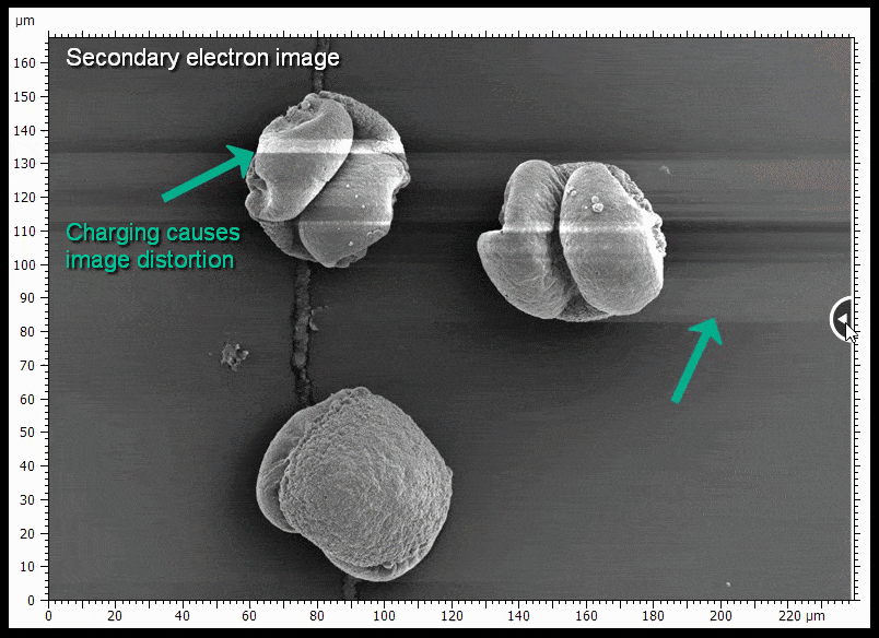
The sample shown is gold coated pine pollen. Some of the pollen grains do not touch the surface very well and charge when being imaged, causing distortions. BSE imaging is less prone to being distorted by charging.
Improve the quality of information in your images
Resolution and image quality are extremely important analysing your data and when you want to publish.
Improve your electron image resolution
- Make sure your column and apertures are correctly aligned and the astigmatism has been corrected using the stigmata. The latter is particularly important for achieving the best resolution. The video below shows how difficult it is to get sharp focus until the stigmata are adjusted.
- Reduce your working distance (the distance between the sample and the objective lens). The lower the working distance the higher the resolution, but this will also affect your field of view, depth of focus and your signal intensity. There is an optimum working distance for most SEMs and the different detectors.
- Lower your accelerating voltage (kV). This will reduce the volume of your specimen beam interaction and ensure that your signal is coming from a small area, but this will also lower your signal and it is important to achieve a balance between your image resolution and signal.
- Slow down your scan speed/increase pixel dwell time. This will improve the amount of signal from your sample and reduce noise. If your sample is drifting or charging a slow scan speed will make this worse. Long pixel dwell times can also cause sample damage.
Improve your EDS maps
- Make sure you are activating the x-ray lines of interest. This may take a little research on your behalf. Typically, you will want to have an accelerating voltage that is just over twice the energy of the x-ray line you are looking for.
- Increasing beam current can make a significant difference to the amount of x-ray yield. Detectors such as the Ultim Extreme work very well with low numbers of x-rays, but smaller EDS detectors or detectors that cannot as close to the sample may need more, which can be achieved by increasing the beam current or the aperture size.
- Increase the number of frames. Acquiring data from biological samples will typically take longer than for materials samples, and acquisition times should be extended accordingly. If your sample is prone to damage or charging, the best way to do this is to acquire more frames. This is particularly important if you are attempting to map very small structures or elements that have a lower concentration.
- Use an appropriate magnification. Make sure that your image resolution and your magnification make sense. There is no point trying to map 10nm gold particles if your pixel size is significantly larger.
- Use an appropriate EDS detector for your research. Most biological EDS can be acquired using the Ultim Extreme detector, which enables you to optimise your image resolution with shorter working distances and low kV, without compromising your EDS data acquisition.
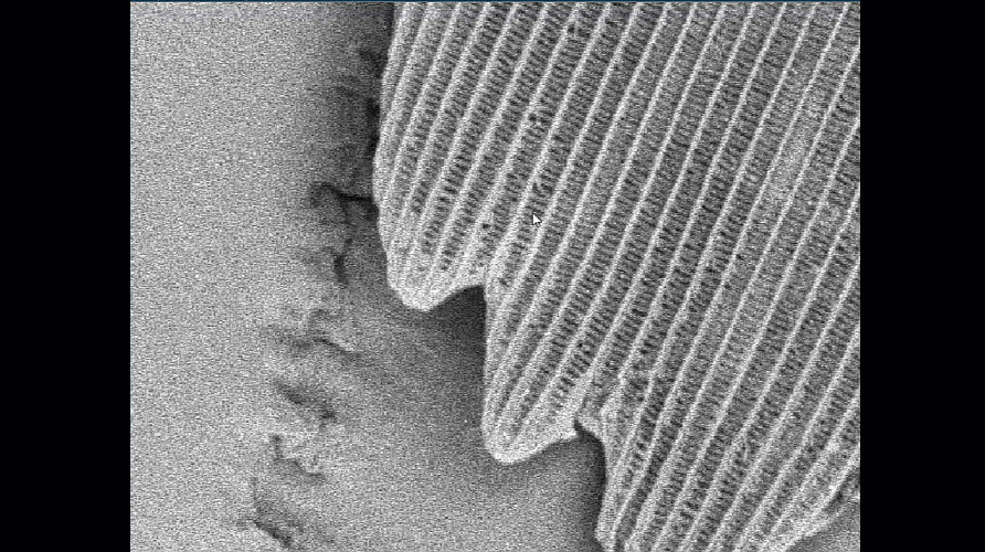
Video shown is of a butterfly wing. Improving the alignment of the column makes a significant difference to the quality of the final image.
Do you have any good tips and tricks for improving your imaging? Comment below
 Part of the Oxford Instruments Group
