Products
FIB-SEM
Nanomanipulators
OmniProbeOmniProbe CryoSoftware
AZtec3DAZtecFeatureAZtec LayerProbeTEM
Hardware
EDSUltim MaxXploreImaging
TEM CamerasSoftware
AZtecTEM
 Part of the Oxford Instruments Group
27th January 2022 | Author: Dr Sam Marks
TEM analysis can be utilised to acquire atomic resolution images and EDS data, typically focussed in the nanoscale, taking advantage of electron transparent samples with thicknesses < 100 nm. Atomic resolution EDS requires aberration corrected microscopes that have been painstakingly aligned to achieve the optimum working conditions for the maximum resolution.
This is a lot of work for great results, however, even standard day to day TEM operation acquiring EDS data and images from 5 - 50 nm features is surprisingly time-consuming. The inability to examine multiple samples, paired with the time it takes to load samples into the column and perform basic beam alignments can be extremely frustrating. Especially if, after the 15 minute setup cycle, you find that your FIB lift out is too thick, from the wrong area or, in the worst case scenario, has fallen off the grid!
An alternative method to TEM analysis is STEM-SEM, in which electron transparent samples can be imaged in the SEM in combination with a STEM detector to perform high resolution imaging and EDS. As the samples analysed are electron transparent, we see a significant improvement in the spatial resolution of the EDS maps, as the effects of interaction volume are minimized. See my previous blog “How should I acquire high-res EDS maps?” for a comparison of interaction volumes for standard SEM, low kV SEM and STEM-SEM.
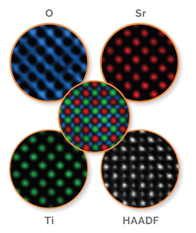
Atomic resolution EDS of STO, acquired using dual Ultim Max TLE detector
A key advantage of STEM-SEM is that the level of beam alignment required for high resolution analysis is significantly lower. Most modern SEMs contain readily available auto alignment routines and high end aberration correction is not required. This makes high resolution imaging and EDS mapping more accessible to microscopists and can be utilised to free up availability on the TEM.
Below you can see examples of STEM-SEM analysis in which an Ultim Extreme windowless detector is being utilised to examine a semiconductor device. In this scenario, we are using an electron microscope with an immersion field so that the windowless EDS detector can be used in combination with high accelerating voltages. Here we have acquired a quick EDS map, over 300 seconds, which clearly shows an extremely small layer of nitrogen, approximately 8 nm thick.
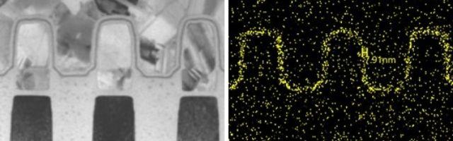
STEM-SEM image of a semiconductor device and corresponding nitrogen EDS map
Further analysis using a linescan highlights that the nitrogen feature is comprised of two independent 4 nm sections.
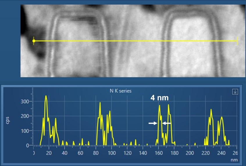
EDS linescans indicate that the 8 nm nitrogen feature is actually two 4 nm features side by side
With STEM-SEM the samples being analysed are no longer bulk, so we see a significant reduction in X-ray count rate, similar to performing EDS at low accelerating voltages. To compensate for this reduction in X-rays, we require either a large area EDS sensor or a high solid angle. In this example, we are utilising the Ultim Extreme detector, a large solid angle detector, which results in great EDS data in a reasonable time frame, without any concerns about sample drift.
It is clear to see why this type of sample is traditionally analysed using TEM, and most microscopists are surprised at the level of resolution that can be achieved using STEM-SEM. The ability to load multiple samples and perform quick automated alignments makes STEM-SEM a viable alternative to TEM for imaging and EDS analysis of samples with features in the 5 – 100 nm range. Wider adoption of STEM-SEM for analysis of samples in the tens of nanometer size scale can result in the freeing up of valuable TEM time.
Dr Sam Marks,
Key Account Manager, Oxford Instruments
Dr Sam Marks graduated with an MPhys in Physics from the University of York, and a PhD in electron microscopy from the University of Warwick. He joined Oxford Instruments in 2018 and has always worked with a strong focus on high resolution electron microscopy. Sam has focused his research on S/TEM, in particular in-situ characterisation. One of his current roles is TEM Product Manager within the EDS Product Marketing Group.
We send out monthly newsletters keeping you up to date with our latest developments such as webinars, new application notes and product updates.
© Oxford Instruments 2024