Introduction
Since its development in 2010–2012, Transmission Kikuchi Diffraction (TKD)* in the scanning electron microscope (SEM) has become an increasingly routine technique for the characterisation of nanostructured materials [1–3]. The simplicity of the TKD technique, involving a standard EBSD system fitted to a field emission gun (FEG) SEM, coupled with a spatial resolution on the scale of 2–10 nm, has enabled researchers to carry out orientation mapping on samples with grain sizes significantly below 50 nm, something that would have been impossible using conventional EBSD.
The key to the improved spatial resolution of TKD is the use of electron transparent samples, such as those prepared for standard transmission electron microscopy (TEM). Unlike in TEM, most commercial SEMs are limited to beam energies of 30 kV, and so there is significantly more electron scattering through the sample thickness when analysing using TKD. This means that the sample thickness is critical: too thick and the electron beam will scatter more broadly and there will be a significant loss of resolution, too thin and there will be insufficient diffracted signal to enable effective and fast measurement. In addition, sample preparation using a focused ion beam (FIB) SEM can result in amorphisation of the sample surface due to Ga ion implantation: as the dominant signal for TKD comes from the lower surface of the sample, Ga-damage can cause complete loss of the diffraction pattern and prevent successful analyses.
AZtecSynergy was used to collect Energy Dispersive X-ray Spectroscopy (EDS) and TKD data. AZtec LayerProbe was used to determine the sample thickness and degree of Ga damage in TEM foils, and to assess the optimum sample thickness for a range of materials. This approach is described and applied to demonstrate the effect of sample thickness and density on TKD results.
* also known as transmission electron backscatter diffraction (t-EBSD)
Method
Three samples were selected for TKD analysis:
- Ultrafine grained TiO2 sample
- Nanostructured NiCo sample deformed at high strain rate
- Naturally deformed diamond sample
TEM foils were prepared either by electropolishing (NiCo) or by FIB-SEM lift-out and thinning (TiO2 and diamond). The diamond sample was supported on a holey carbon support film and the TiO2 sample was welded to an OmniProbe Cu support grid. All 3 samples were then mounted using a stainless steel sample holder in such a way that they were horizontal in the SEM chamber at a level just above the EBSD detector phosphor screen, and close to the optimum working distance for EDS (approximately 8 mm in this set up). It is important that the material used for the support grids and the sample holder is not the same as the elements found in the samples.
A NordlysNano EBSD detector and an X-Max 20 mm2 EDS detector coupled with AZtec software were used for data acquisition. The NordlysNano detector is optimised for sensitivity and is therefore the best detector for this application. A forescatter electron detector (FSD) was used to generate darkfield images of the samples in order to visualise thickness variations and to assess sample quality.
The electron beam was set to 30 kV, with a current of 5–10 nA in a depth of field mode. The samples were cleaned for 5 minutes using an on-chamber plasma cleaner and then a reference EDS spectrum was collected from the Cu support grid in order to calibrate the beam current for subsequent thickness measurements.
TKD maps were collected using step sizes of 20 nm (TiO2 sample) and 10 nm (NiCo sample) along with simultaneous EDS measurements, at a rate of ~41 points/second. Autolock drift correction was used during the long (7 hours) analysis of the NiCo sample. The diamond sample was analysed by collecting TKD patterns and EDS spectra at individual points. Sample thickness measurements were calculated offline by extracting spectra at regularly spaced positions from the maps and processing them using AZtec LayerProbe.
Results
1. Ultra Fine-Grained TiO2
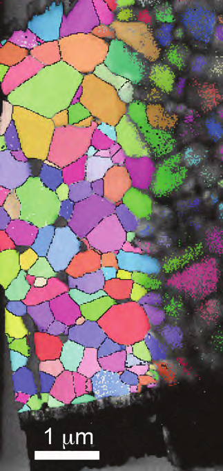
During FIB preparation, the foil was thinned in 2 stages, with one part of the section thinned down to a greater extent. The TKD mapping showed that in the thinnest region, pattern quality was extremely high and almost all points (with the exception of the voids) were easily indexed. However, in the thicker region, the pattern quality was significantly poorer and indexing was only possible in the centres of the grains.
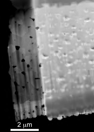
Fig. 1. Forescatter electron dark field image of FIB-prepared TiO2 section.
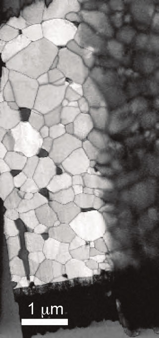
Fig. 2a. TKD pattern quality map (band contrast).
 T
T
Fig. 2a. Unprocessed TKD orientation map (IPF-x) with high angle boundaries in black.
The LayerProbe results show the significant contrast in thickness between the 2 regions: in the area producing good diffraction patterns and successful indexing, the TiO2 is between 50 and 150 nm thick with less than 1 nm of detected Ga implantation. However, in the thicker region the TiO2 is between 300 and 600 nm thick — enough to cause significant beam broadening and an associated loss of TKD resolution. In this foil, cleaned with a final low kV ion beam polish in the FIB, there is little sign of any Ga implantation except at the very bottom of the foil, likely caused by sputtering and redeposition from the OmniProbe grid.
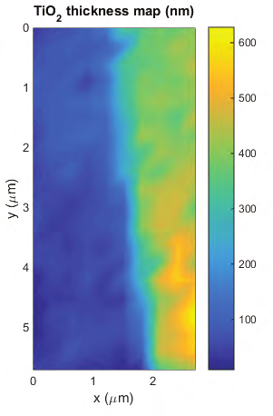
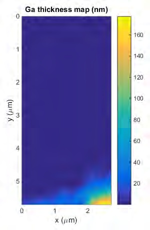
Fig. 3. Thickness maps.
2. Deformed NiCo Sample
An area of ~14 µm × 7 µm extending away from the edge of the electropolished foil was analysed in the deformed NiCo sample. The FSD darkfield image shows numerous holes in the foil adjacent to the edge, and a gradual increase in foil thickness towards the lower right corner. This increase is reflected in the pattern quality map with a noticeable decrease in pattern quality and blurring of the grain boundaries in the thickest region. Despite this, the unprocessed orientation map shows excellent indexing throughout the analysis area, giving a mean grain size of 172 ± 2.3 nm.
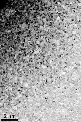
Fig. 4. FSD darkfield image of the NiCo analysis area.
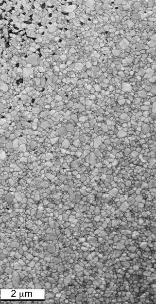
Fig. 5a. TKD pattern quality map (band contrast).
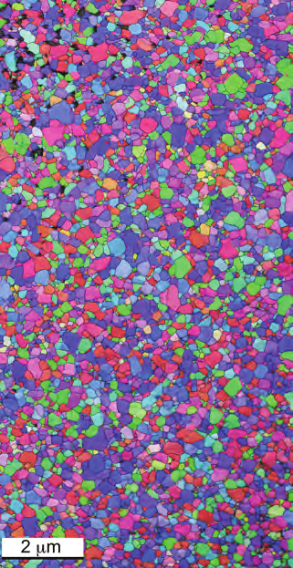
Fig. 5b. Unprocessed TKD orientation map (IPF-x), with high angle boundaries in black and CSL boundaries in colour.
The LayerProbe thickness results indicate a gradual change from <40 nm thickness adjacent to the foil edge, to >120 nm thickness in the lower right corner of the analysis area. The detailed pattern quality maps demonstrate the corresponding impact on the TKD results. The map taken from the centre of the dataset, with a mean specimen thickness of 68 nm, shows TKD patterns that are extremely good, resulting in >96% indexing with only a few non-indexed points along the grain boundaries. The map taken from the thickest region, with a mean thickness of 118 nm, shows that electron scattering significantly decreases the TKD spatial resolution, resulting in many more unindexed points at the grain boundaries (the total indexing drops to 87%).
Despite the significant worsening in spatial resolution in the thickest region of this analysis, the TKD indexing rate is still sufficient to enable accurate determination of the grain size and grain boundary characteristics. However, for the best spatial resolution and for effective characterisation of even finer grained NiCo samples, these data suggest that an optimum sample thickness would be in the range of 40–70 nm.
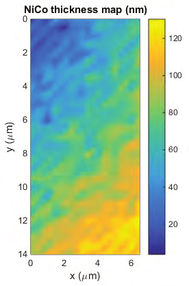
Fig. 6. Thickness map
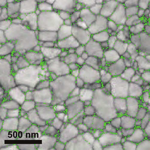
Fig. 7a. TKD pattern quality map from a central area within the dataset (thickness 68nm), with non-indexed points shown in green
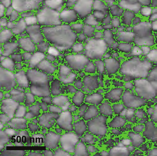
Fig. 7b. TKD pattern quality map from a lower right area within the dataset (thickness 118nm), with non-indexed points shown in green.
3. Diamond
For low atomic number (Z) materials, such as diamond, thicker samples are generally required in order to generate enough diffracted signal; an additional problem is the occurrence of diffraction spots in the lower part of the TKD pattern, especially in the thinnest regions. These spots can be seen in all of the example TKD patterns below, but they only affect the automated band detection in the pattern from a 29 nm thick region. In the thicker regions (measured as 82 nm and 110 nm thick using LayerProbe), the diffraction spots are visible but do not affect the Hough transform used for band detection. Indexing was possible in all 3 regions, as strong Kikuchi bands were detected away from the diffraction spots, illustrating the advantage of using an off-axis detector.
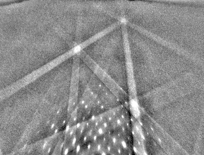
Fig. 8a. Diamond TKD pattern – 29nm thickness.
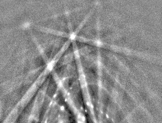
Fig. 8b. Diamond TKD pattern – 82nm thickness.
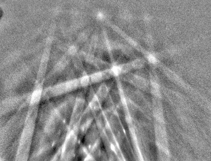
Fig. 8c. Diamond TKD pattern – 110nm thickness.
It is clear from these patterns that a thickness greater than 100 nm is ideal for TKD analyses of low Z samples although, for truly nanocrystalline or highly deformed structures, the ability to work with thinner samples and to minimise the effect of diffraction spots would be advantageous.
Summary
The effectiveness of TKD for characterising nanocrystalline samples is strongly dependent on sample density and thickness. The combination of TKD, EDS and AZtec LayerProbe allows us to determine the thickness of samples quickly and accurately, as well as to determine the extent of beam damage from ion beam sample preparation. Here we demonstrate the versatility of the technique on 3 contrasting samples: a FIB-prepared TiO2 sample in which the optimum thickness is shown to be between 50 and 150 nm, an electropolished NiCo sample that shows ideal pattern quality in regions under 80 nm thick and a diamond sample in which diffraction spots become prominent in the thinnest regions, <50 nm thickness.
This additional analytical capability is a significant benefit when preparing samples in the FIB, as well as for the selection of optimal areas for subsequent, high-resolution TKD analyses.
Acknowledgements
Sandra Piazolo and Zibin Chen are thanked for providing samples and Glenn Sneddon helped with the LayerProbe thickness maps. All analyses were carried out at the Australian Centre for Microscopy & Microanalysis at the University of Sydney. Oxford Instruments thanks Pat Trimby for his help in producing this application note.
References
- R.R. Keller and R.H. Geiss, J. Microscopy 245 (2012), 245–251
- P.W. Trimby, Ultramicroscopy 120 (2012), 16–24
- P.W. Trimby et al., Acta Materialia, 62 (2014), 69–80

