High-resolution TEM image quality is greatly impacted by the thickness of the TEM sample (lamella) and the presence of any surface damage layer created during FIB-SEM sample preparation. Here we present a new technique that enables measurement of the local thickness and composition of TEM lamellae and discuss its application to the failure analysis of semiconductor devices. The local thickness in different device regions is accurately measured based on the X-ray emission excited by the electron beam in the FIB-SEM. Examples using this method to guide FIB-SEM preparation of high quality lamellae and to characterise redeposition are shown for Si and III-V semiconductor devices. We also show how high quality data can be obtained while analysing the sample held on the tip of an OmniProbe 400.
1. Introduction
Over the last twenty years, FIB-SEM techniques have become the preferred method for site-specific TEM sample preparation in large part due to their high resolution capabilities for imaging and milling. In order to take full advantage of the ever increasing resolution in aberration-corrected TEMs, control of the sample quality and thickness has become paramount. Accurately achieving a desired lamella thickness and minimising any amorphisation caused by ion implantation, all while ensuring a high throughput of samples, is very challenging. The lamella thickness is usually estimated by imaging the lamella edge-on. However, this method hides any local thickness variations, some of which can be substantial. For FIB-SEM instruments, more sophisticated lamella thickness endpoint detection methods based on either back-scattered electron contrast [1] or transmissivity of electrons [2] have been demonstrated where the lamella is imaged in the plane normal to the electron beam. However, these methods only work on homogenous samples lacking compositional variations and require the contrast to be calibrated using the same material. They also don't provide any information on ion implantation or surface amorphisation, which can greatly affect the quality of the TEM image obtainable from the lamella.
Here we show a method that uses X-rays generated by the electron beam - lamella interaction to accurately and rapidly measure the lamella composition and thickness, including measurements of the damage layer induced by Ga+ ion implantation. A similar method has been used to measure a wide range of thin films and layers on bulk substrates [3]. We also discuss the possibility of analysing and thinning a sample while on the tip as a possible method to speed up sample preparation and minimise Ga+ ion implantation.
2. Method
In situ lift out of the lamella using a nano-manipulator generally has a higher success rate than ex-situ lift-out but can take longer and uses FIB time. It is therefore often reserved for precious samples where fault isolation has been difficult, or for samples that require advanced preparation such as backside lamella thinning. During sample transfer from the FIB to the TEM or vice versa, there is risk of losing or damaging a lamella. Ideally there is only one transfer step from FIB to TEM. However, in some cases multiple transfers happen because either a) during TEM analysis it is discovered the desired thickness was not achieved, mandating rethinning or b) sample retention is so critical, TEM imaging is performed as a confirmatory step to localize the target within the lamella and ensure the final site is not lost due to overmilling. To minimise the need to transfer the sample between FIB and TEM and to improve sample throughput we demonstrate a method that involves (1) Rapid milling of the sample in the trench to a thickness of around 1 micron, (2) Rapid further thinning of the sample on the manipulator tip or on the grid close to electron transparency and (3) a final thinning and clean-up on the grid. We show that the intermediate thinning step (2) on the manipulator leads to a significantly reduced Ga concentration when compared to thinning in the trench.
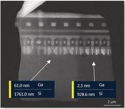
Fig. 1 — Electron image of a lamella, the right side of which has been thinned while being held on the manipulator tip. Measurements of the thickness and Ga content are also shown.
In order to monitor the Ga implantation and to quantify the thickness and composition of the lamella at each step, we used Oxford Instruments' AZtec LayerProbe software and X-Max EDS detectors to acquire and process EDS spectra. The LayerProbe software refines a starting model of the sample structure against the EDS spectra to calculate the film thickness and composition of the layers. The starting model comprises the layer sequence in the sample and a substrate material. As the TEM lamella is a free-standing layer the substrate is defined as comprising an element that is not contained in the lamella and only weakly scatters electrons such as beryllium. The first layer is defined as the material comprising the lamella and its thickness is used as a measure for the lamella thickness. The top layer can be defined to contain the element used as the ion source (e.g. gallium) to obtain a measure of the degree of ion implantation in the specimen.
For the lamella lift-out and on-tip thinning an OmniProbe 400 nanomanipulator was used. This latest-generation nanomanipulator is optimised to minimise drift and vibrations and therefore enables imaging and analysis of the sample on-tip at high resolution.
3. Experimental Results
3.1 Thickness measurement and thinning on the manipulator tip
For standard TEM lamella preparation, the manipulator is used to transport the lamella from the original site on the chip onto a lift-out grid, which can then be put into the TEM. The sample is usually only imaged at relatively low magnification while held by the manipulator, while more detailed analysis has been challenging due to vibration and drift. However, on-tip sample analysis has a number of advantages over on-grid analysis, including easy lamella positioning in the chamber so that there is no secondary signal from the grid or holder (which may be the case if the lamella is thin enough for a significant part of the electron beam to be transmitted).
Fig. 1 shows a lifted-out lamella which has been welded to the manipulator tip (left upper corner). The right hand side of the lamella was thinned while on the tip. Subsequently EDS spectra were acquired from both areas in regions of pure Si. The LayerProbe measurement confirms that the thickness was reduced by about half. The measurement also shows a significant decrease in the Ga concentration even though the milling conditions were the same as when milling in the trench and no low-kV clean-up step was used.
Fig. 2(a) shows an X-ray map of the device region before further thinning. It is recorded with a beam accelerating voltage of 30kV. At this voltage the beam is expected to fully penetrate even the thicker region of the lamella, so the sample thickness clearly determines the X-ray map resolution, with the thinner area showing more clearly defined Cu features. However, the smaller W structures seen in the electron image are still not well-defined at a sample thickness of just under 1 micron. Nitride layers of about 50nm thickness cannot be resolved at all. Further thinning to about 300nm thickness (Fig. 2(b)) provides a much clearer definition of the W device regions and clearly shows a nitrogen signal at the location above the copper.
This not only shows the capability of the X-ray method for guiding thinning on the tip, but also opens up the possibility to perform on-tip analysis, replacing TEM for applications where the maximum required EDS resolution is around 50nm. As the lamella gets thinner, the X-ray yield drops. However, with a large area EDS detector like the X-Max 80 which acquired the map in Fig. 2, sufficient mapping data can still be acquired in a matter of minutes. In fact, spectra with sufficient number of counts to perform point measurements of the lamella composition and thickness can be acquired in less than 10 seconds.
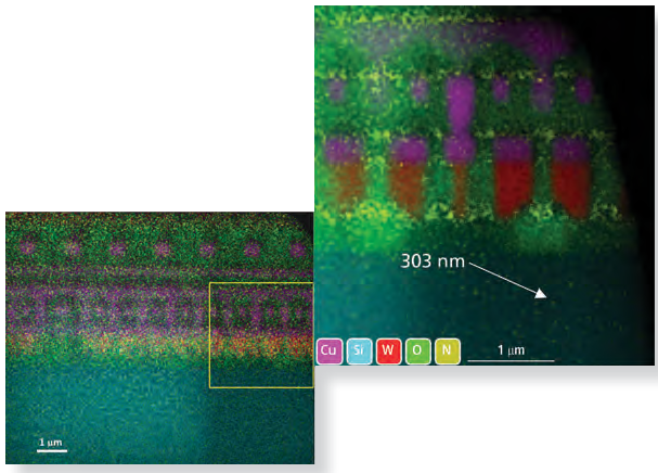
Fig. 2 — (a) Shows an X-ray map of the device region of the sample from Fig. 1. (b) shows the region enclosed by a square in (a) after further thinning.
3.2 Thickness measurement and thinning on the grid
If a manipulator of sufficient vibrational and drift stability to carry out on-tip analysis is not available, X-ray analysis of the lamella thickness and guided thinning can still be carried out by welding the lamella to a TEM grid. Fig. 3a shows a lamella welded to a Cu grid post. The right hand side of the lamella has been thinned until a hole appeared in the lower half of the lamella. Thickness values measured with LayerProbe in different regions of the lamella are shown in white on the lamella. Close to the hole a lamella thickness below 20nm was measured which increased significantly further away from the hole. In the copper lines towards the top of the lamella the highest measured thickness was 130nm, indicating a significant variation in thickness over the lamella area.
The measurement also shows that LayerProbe is capable of measuring sample thicknesses well below 50nm which is critical for preparing ultra-thin TEM lamellas.
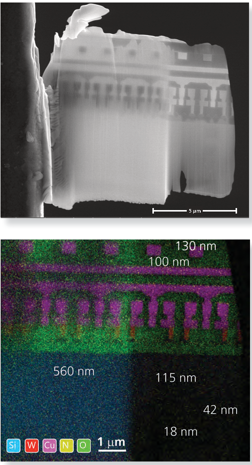
Fig. 3 — (a) Shows the electron image and (b) the X-ray map of a lamella which was thinned on the grid. Local thickness measurements are shown in white letters.
3.3 Multiple layers within the lamella depth
Fig. 4 shows an X-ray map of a TEM lamella prepared from a silicon semiconductor device. The device structures containing Cu and W are clearly visible in the X-ray maps. One of the Cu lines fades and disappears from the right side to the left of the lamella. This indicates that the line runs at an angle to the direction of the FIB cut. With LayerProbe it is possible to measure the projected Cu thickness and Si thickness from X-ray spectra reconstructed from the X-ray map. By comparing measurements taken from the right side of the lamella with measurements towards the left side we can see how the thickness increase of the lamella affects the ratio of device vs surrounding Si matrix for both the W and Cu rich device areas.
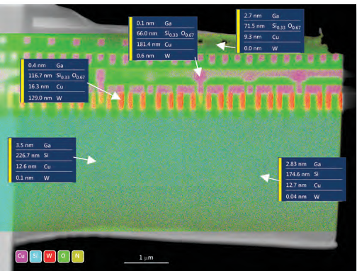
Fig. 4 — Measurements of the local lamella thickness as well as the contribution of different device layers.
3.4 AlGaAs VCSEL
In order to further investigate the capability of measuring samples with local compositional and structural variations, measurements were taken from a lamella prepared from a VCSEL structure. The lamella contains all device areas of interest in the VCSEL including the reflectors (alternating AlAs and GaAs), the top contacts (Au and Mo) and the GaAs wafer at the bottom of the lamella. The lamella was deliberately prepared as a wedge shape with the thickness increasing from top to bottom in order to test the ability to deal with large thickness variations. To calculate the thickness and composition, the LayerProbe model was adapted for each area of the VCSEL. For measurements in the reflector areas the model was defined as AlxGayAsz/Be, with the Al, Ga and As content as well as layer thickness set as unknowns to be calculated. The model was set up as Au/Be for the Au contact and as GaxAsy/Be for the substrate area. The thickness measurements obtained from different points on the lamella clearly show the increase in thickness from the GaAs substrate towards the top of the lamella. At the base a thickness of 850nm was measured, whereas in the Au contacts, the measured thickness was only about 300nm (Fig. 5). At the same time as measuring the thickness, LayerProbe was also used to determine the composition in the different regions of the VCSEL. For the substrate the measurement confirmed the stoichiometric 1:1 composition of the GaAs wafer. In the top half of the quantum wells region the Ga:Al ratio was about 1:1 whereas towards the base of the lamella this ratio was closer to 2:3. Closer investigation of the quantum wells in an FE-SEM showed that the AlAs regions were indeed broader than the GaAs layers, which explains the change in the Ga:Al ratio throughout the reflector region.
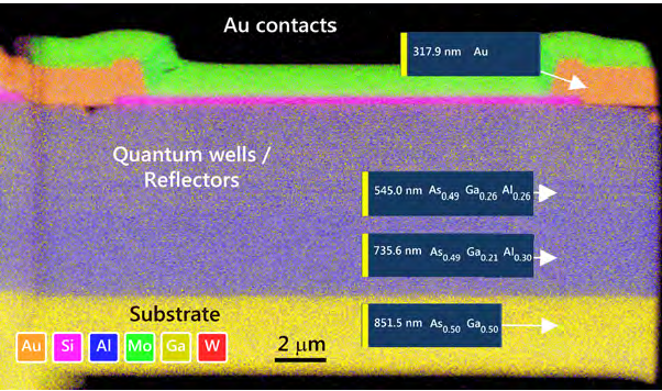
Fig. 5 — Shows an X-ray map of an AlGaAs VCSEL together with thickness measurements from different areas in the sample.
4. Applications in Failure Analysis
Our initial experiments show how LayerProbe can be employed to measure the local lamella thickness and composition. As device structures are getting smaller, the ability to endpoint the specimen thinning on individual semiconductor devices and even regions within a device becomes more important. As the lateral spatial resolution of a LayerProbe measurement is on the same order as the lamella thickness, this opens up the possibility to direct the local thinning of selected device regions on the lamella. We expect that locally directed thinning will enable clearer TEM images and better analysis of the failed devices and increase the yield of successfully prepared TEM lamellas. As LayerProbe also measures the Ga content in the lamella it can be used to quantify the Ga implantation from the ion beam. This provides a measure for surface damage due to amorphisation by the Ga beam. The amorphised surface layer needs to be removed either in the FIB-SEM or by other methods in order to obtain high quality TEM images or analytical results. The ability to measure the presence and thickness of such a surface layer can be used to monitor its successful removal.
As most FIB-SEMs are already equipped with an EDS detector, no additional hardware is necessary to implement local thickness and compositional measurements using this new technique. We expect that this will enable its rapid adaptation as a standard metrology tool to support the preparation of high quality TEM lamellas for failure analysis.
We also showed that both milling and high resolution X-ray analysis on the manipulator tip are possible if the nanomanipulator construction is designed to dampen vibrations and control drift. In combination with large area X-ray detectors which maximise the number of X-ray counts captured from thin samples, this may well enable more failure analysis tasks to be performed directly in the FIB-SEM. This is a path to reduce the reliance on TEM analysis with the exception of tasks needing very high spatial resolution.
References
- [1] Hall A. R. Microscopy and Microanalysis
- 19 (2013) 740–741.
- [2] Golla-Schindler U. Conference Proceedings EMC (2008) 667–670.
- [3] Lang C. et al. Microscopy and Microanalysis
- 19 (2013) 1872–1873.

