Introduction
Research and development of electronic circuitry mounted on plastic substrates is gathering pace with an increasingly large range of products incorporating flexible components. Such circuits are increasingly found in consumer electronics, medical devices, automotive settings and in satellites. In order to assess the structural properties of the electronic components, they have to be analysed while on the plastic substrate without compromising their structural integrity. LayerProbe enables the analyst to separate the contributions of the substrate and the structures and enables measurements of the thickness and composition at high resolution and in a non-destructive manner.
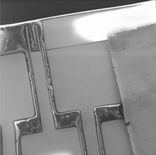
SE image showing gold contacts (mid-grey, flat areas), polymer substrate (channels) and Cu tape.
Measuring Circuitry on Glucose Testing Strips
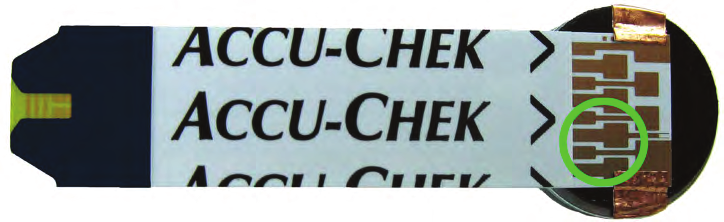
Here we show how LayerProbe can be used to analyse the circuitry found on a commercially available glucose test strip.
A glucose testing strip causes a small sample of blood to come into contact with an enzyme which promotes an electrochemical reaction when glucose is present. The result is that a current flows when glucose is present within the blood sample and the size of the current is proportional to the amount of glucose present. As such, it is very important that the thickness of the metal circuitry which transports the current from the point at which it is generated by the enzyme to the contacts which connect to the electronic reader is consistent. This is because variations in the thickness will alter the current and so may potentially cause incorrect readings of blood sugar to be recorded with potentially serious consequences for the patient.
Analysis
The circuitry of the glucose testing strips investigated here consists of gold contacts deposited on top of a polymer base. Here, we have analysed the end of the testing strip which attaches to the measurement device where the gold contacts are exposed, enabling their analysis without further sample preparation.
A model of the testing strip is defined for LayerProbe analysis. EDS spectra obtained from the polymer substrate show that it consists of C, O, Ba and S. BaSO4 is commonly used as a white coloured filler and carbon and oxygen are the main constituents of the polymer. Thus, the model can be defined as:
| Layer | Nominal Composition | Composition Known/Unknown | Nominal Thickness | Thickness Known/Unknown |
| Layer 1 | Au | Known | 50nm | Unknown |
| Substrate | COBaS | Unknown | Substrate | Substrate |
Using LayerProbe's "Set up Solver" it is possible to determine which accelerating voltage should be used to ensure that both the Au layer and the substrate are effectively sampled and all of the elements present are excited. This solubility calculation takes into account all parameters of the model as if they are true (e.g. nominal thickness values are used to determine the excitation volume required). In this case the results of the solubility calculation suggest that an accelerating voltage of 20kV will give the best results for the Au layer thickness measurement whereas a value of 30kV would be best for determining the composition of the substrate. Here the parameter of primary interest is the thickness of the Au layer and as such, an accelerating voltage of 20kV was chosen.
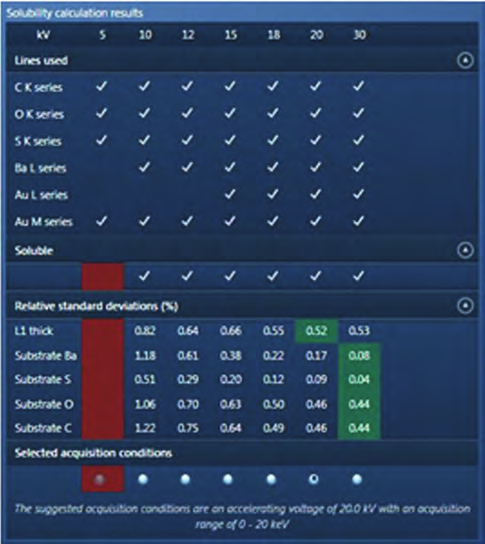
Set up solver solubility calculation results suggesting at which accelerating voltage the problem is solvable and the relative standard deviations which can be expected for the data for each of those solutions.
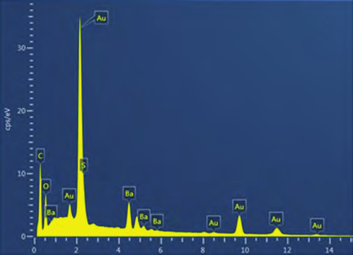
Spectrum obtained from Au contact and calculated LayerProbe results. Au is calculated as 45.8nm.
Once ideal acquisition conditions had been determined, measurements were recorded across the sample (see figure below). The spectra were imported into AZtec and processed with LayerProbe using the model and x-ray line selections which had previously been determined. The results were then plotted as a surface using MS Excel. This method of plotting is particularly useful as it allows layer continuity and consistency to be intuitively viewed. The results show that the thickness of the Au layer varied over a range of 3nm across the area sampled.
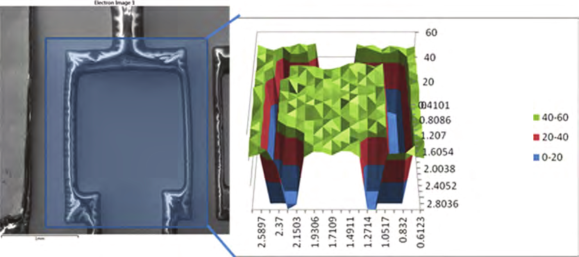
Electron image showing acquisition area and surface plot showing thickness of Au layer recorded across that area. The area with the irregular texture in the electron image is the polymer which forms the structure of the strip