Introduction
Development and testing of semiconductor devices requires extensive knowledge of local structure and elemental composition. With feature sizes of <5 nm, it is often necessary to perform imaging and EDS analysis in a S/TEM.
Once in the TEM, there are still many difficulties to be overcome to acquire accurate elemental maps. Elemental analysis of semiconductors is typically difficult due to strong overlaps of X-ray lines between commonly used elements and low concentrations of dopants. Not only are concentrations of dopants small but their X-ray lines often overlap with other materials used in semiconductor processing. This brief shows how AZtecTEM solves these overlaps to achieve an accurate elemental analysis.
Solving for Overlaps
Traditionally, EDS maps are generated using a 'window integral' approach that sums the area of each peak in the spectrum to identify the elements that are present and their concentration. However, this approach is prone to significant errors, especially when peak overlaps occur. AZtecTEM TruMap overcomes these limitations. Using a 'deconvolution' approach, elemental peak shapes are fitted across the entire spectrum for each pixel in the EDS map. TruMap associates X-ray counts with the right element in the right location in real-time.
Example of Overlaps
- Si K and W M lines — 1.74 keV and 1.77 keV
- Cu K, Ta L and Hf L lines — 8.05 keV, 8.15 keV and 7.90 keV
- As L and Ta M lines — 1.28 keV and 1.33 keV
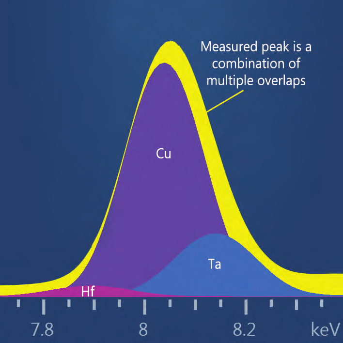
Figure (above) shows overlaps occur for elements that are commonly used in semiconductors. AZtecTEM TruMap solves these problems in real-time (below).
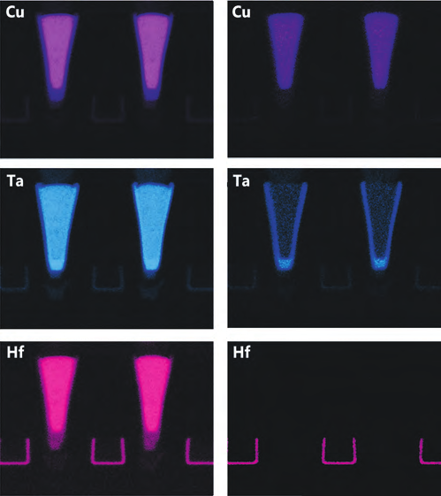
Traditional approach on the left: Cu, Ta, Hf look the same
Aztec TruMap: elements clearly resolved
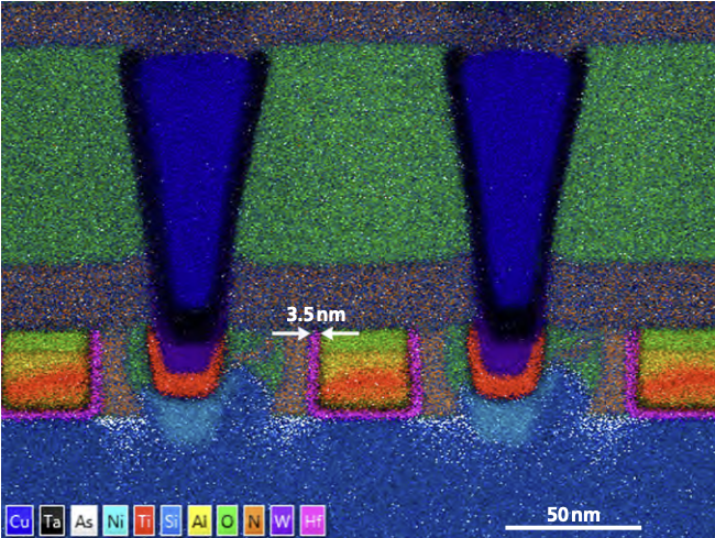
QuantMap of a modern FINFET transistor. Hf structures of 3.5 nm are accurately mapped. The strong Cu–Ta overlap is successfully deconvolved and then mapped to show distinct regions of Cu and Ta. As dopants of 0.1 weight% are separated from their own strong Ta overlap and are clearly visible.
QuantMap in AZtecTEM goes one step further and displays real quantitative chemical X-ray maps. By recalculating the original map data — and correcting for X-ray background, peak overlaps and pile-up artefacts — QuantMaps can be calculated on-line during acquisition. QuantMap allows mapping by weight%, atomic%, or oxide% using the well established Cliff-Lorimer method.
Even dopant concentrations as small as 0.1 weight% can be accurately mapped using Ultim Max and AZtecTEM.
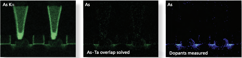
The three steps of AZtecTEM: window integral mapping, peak deconvolution using TruMap, and finally measurement using QuantMap.
Conclusion
Thin sections of semiconductor specimens can now be accurately mapped in real time using Ultim Max windowless EDS detectors for TEM. Used in conjunction with AZtecTEM and TruMap, common elemental overlaps such as Si K and W M lines are easily solved. Elements are not just mapped but can also be quantified using QuantMap giving accurate measurement of dopant and even oxide concentrations.

