Introduction
Beam-sensitive materials are challenging to study in an electron microscope. This is particularly so when analysing using the EBSD technique, as the relatively long dwell time required at each pixel coupled with a high probe current and beam energy can easily result in significant sample damage. The solution is often to scan using lower accelerating voltages, typically 8–15 kV, but even then the longer exposure times required to collect good quality EBSD patterns make analyses prohibitively time consuming. Shell nacre, the sub-micrometre scale layering of aragonite crystals found in many mollusc shells, is one of the most challenging of sensitive materials.
There are very few, if any, published EBSD datasets showing effective measurement of shell nacre. Not only is aragonite (and the associated polymorph of CaCO3, calcite) beam sensitive, but the fine scale of the structures requires a measurement spacing in the order of 100 nm to ensure good resolution of the nacre layers. Such a small step size invariably results in cumulative damage to the aragonite crystals, rendering effective analyses almost impossible.
The Symmetry EBSD detector, based on optimised CMOS technology, dramatically enhances the capabilities of EBSD to analyse sensitive materials. Here we compare datasets collected using the same field emission gun SEM from the shell of the common mussel, Mytilus edulis, using an existing sensitive CCD-based detector and using Symmetry.
Results
In both cases, the interface between prismatic calcite and the aragonite nacre has been scanned. In the analysis using a conventional CCD detector, the accelerating voltage was 15 kV and the measurement step size was 167 nm. Patterns were exposed for 89 ms using a probe current of 1.5 nA. Using Symmetry, the accelerating voltage was 12 kV and the step size was 60 nm. However, patterns were only exposed for 2.5 ms using a probe current of 7.8 nA. The electron dose of both measurements, expressed in terms of (nA x s) / μm2, was broadly similar (4.81 and 5.47 nAs / μm2).
The greater sensitivity and speed of Symmetry has enabled a similar area to be mapped much more quickly, with greater spatial resolution and with higher quality indexing, yet exposing the sample to the same dose as when mapped with a conventional CCD detector. These results are compared, for approximately the same sized area, in Fig. 1.
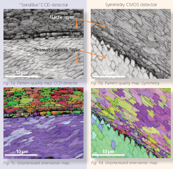
Fig. 1 — Pattern quality maps (Figs. 1a and 1b) and unprocessed orientation maps (Figs. 1c and 1d) comparing the "Sensitive" CCD detector (left) and Symmetry CMOS detector (right), showing the nacre layer and prismatic calcite layer interface in Mytilus edulis shell.
The results in Fig. 1 show how Symmetry produces significantly superior data from this challenging sample in less than 25% of the time. Even the finest nacre layers, in places only 250–300 nm thick, have been resolved (Fig. 1d), thus enabling a complete characterisation of this remarkable microstructure. The speed of analysis enables a much larger area to be measured: the map shown in Fig. 2 was collected in 1 hour and 5 minutes (> 1.5 million measurements at 396 patterns per second) with 97% indexing, without the need for any post-acquisition filtering or image processing.
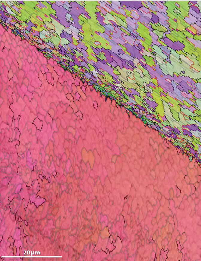
Fig. 2 — IPF orientation map (cleaned), showing high angle boundaries in black and low angle boundaries in grey. In aragonite, special boundaries are marked in red (63.8° <001>) and yellow (52.4° <001>).
Conclusion
The extreme sensitivity and speed of the Symmetry detector makes the effective measurement of nanoscale beam-sensitive materials a possibility. Comparisons with previous studies on the same shell structures using conventional CCD-based detectors illustrate how, for the same electron dose on the sample, Symmetry provides a 7-fold increase in data throughput, enabling higher resolution measurements without any sample damage. This is primarily because Symmetry can collect the required high resolution patterns in millisecond timeframes, ensuring good indexing as well as manageable electron doses. The analysis of 300–500 nm wide aragonite nacre layers can now become routine.

