Introduction
Ever since CCD-based EBSD detectors became commercially available about 15 years ago, the live acquisition speeds of EBSD systems have progressively increased. The latest CCD-based detectors can now acquire diffraction patterns at astonishing rates in excess of 1500 patterns per second (pps). However, this speed comes with a penalty: these rates are achieved by extreme pixel binning, with patterns from a 640 x 480 pixel camera reduced down to a mere 40 x 30 pixels and this can affect the quality of the resulting data.
Utilising a customised CMOS-sensor, Symmetry does not require extreme pixel binning to achieve high acquisition rates. The highest speeds, in excess of 3000 pps, are achieved with a relatively high pattern resolution of 156 x 128 pixels. Even 622 x 512 pixel patterns can be collected and indexed at speeds well in excess of 500 pps. The advantages of this additional pattern information are not only improved hit rates and better phase discrimination, but also a significant improvement in angular resolution.
This technical bulletin explains the effect of this unique combination of speed and pattern detail: the Symmetry advantage.
The Effect of Pattern Resolution
The Symmetry CMOS-based EBSD detector works in a fundamentally different way to a traditional CCD-based detector. In effect, changing pattern resolution has little influence on the speed of acquisition: this means that high resolution patterns can be acquired at very high speeds, something that simply was not possible with CCD-based detectors.
For example, the patterns in Fig. 1 were collected using Symmetry from a duplex stainless steel sample, operating with a beam current of ~10 nA, at a full resolution of 1244 x 1024 pixels. As the speed is increased from 10 pps to 250 pps, the megapixel detail remains but the patterns simply become noisier.
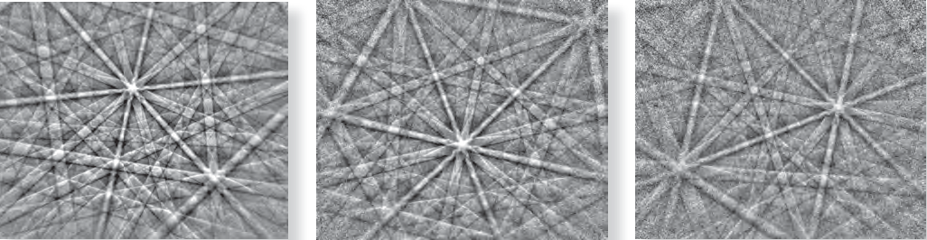
Fig. 1 — EBSPs collected at full resolution (1244 x 1024 pixels) from a duplex stainless steel at ~10 nA probe current. Left – 10 pps, centre – 100 pps, right – 250 pps.
In fact, the only reason to reduce the pattern resolution from Symmetry's full 1244 x 1024 pixels is to enable the software to process and to index each pattern in a shorter time. Reducing the pattern size to 156 x 128 pixels enables AZtec® to perform background correction, band detection and indexing within less than 300 μs (i.e. at speeds well in excess of 3000 pps). However, even a pattern at this resolution contains significant detail, as can be seen in Fig. 2.
In Fig. 2, the heavily binned pattern from a CCD-based detector (left) has barely-distinguishable Kikuchi bands, even from a relatively easy material such as this Ni-based superalloy. For more challenging materials, or heavily deformed samples, the pattern quality becomes so poor that indexing hit rates drop off significantly. This has resulted in the development of pattern averaging techniques in an attempt to compensate for this problem, in effect smoothing the data and losing information on the pixel scale. The equivalent pattern collected using Symmetry has more than 16 times more pixels and is collected in approximately half the time. The band edges are clearly defined, and the indexing process is dramatically improved as a result – not only in terms of the hit rate, but also in terms of the angular precision of the solution. The benefits also extend to more challenging samples, enabling good indexing at high acquisition speeds without recourse to pattern averaging techniques.
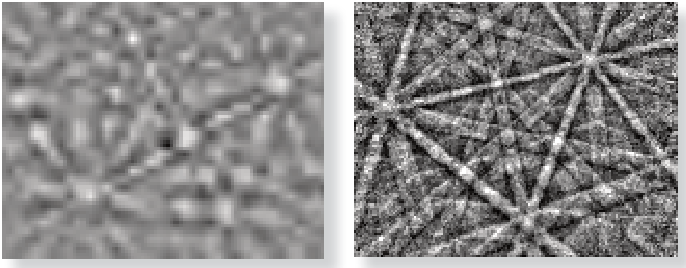
Fig. 2 — Example EBSPs from a Ni-based superalloy collected at maximum acquisition rates (beam current 10 nA). Left – fast CCD-based detector (40 x 30 pixels at 1580 pps). Right – Symmetry CMOS detector (156 x 128 pixels at 3000 pps).
Examples
The benefits of higher pattern resolution are clearly shown in the first example, a partially-recrystallised Ni-based superalloy sample. The same sample was analysed using a traditional CCD-based detector operating at 1580 pps (94.5% hit rate) and the Symmetry detector at 3000 pps (99.2% hit rate). Analytical conditions were approximately the same for both scans. Kernel average misorientation (KAM) maps from both analyses are shown in Fig. 3: these maps provide an indication of the local change in orientation around each pixel, either as a result of sample deformation or the orientation "noise" associated with each measurement. The two maps have the same scale (see inset legend), and show that the KAM values for the measurement using Symmetry are consistently much lower than those collected using the CCD-based detector.
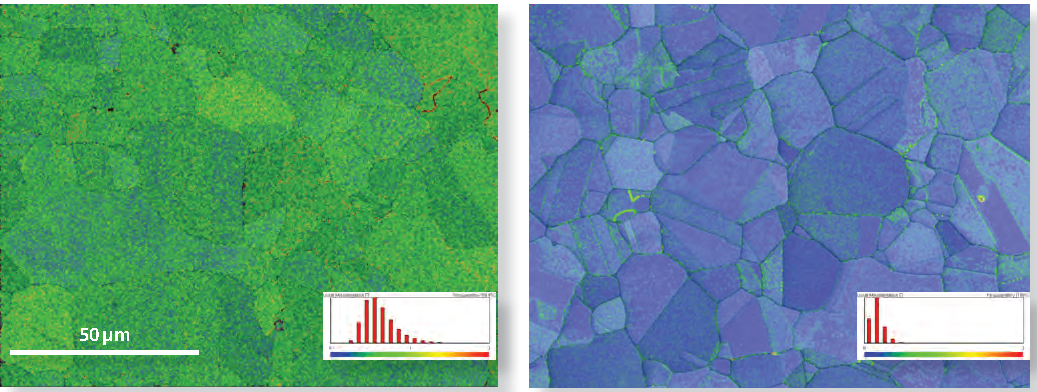
Fig. 3 — Kernel Average Misorientation (KAM) maps from analyses of the same Ni-based superalloy sample. Left – CCD-based detector 1580 pps, right – Symmetry CMOS detector at 3000 pps. Both scales are the same, showing variation from 0 to 2°.
Fig. 4 compares the values from these two maps in more detail. The higher pattern detail from Symmetry has clearly resulted in a dramatic improvement in the angular precision of the data, with the mean KAM value dropping from 0.62° (CCD) to 0.16° (Symmetry CMOS), and with a similar improvement in the variance of the two datasets (0.0491 improving to 0.0097).
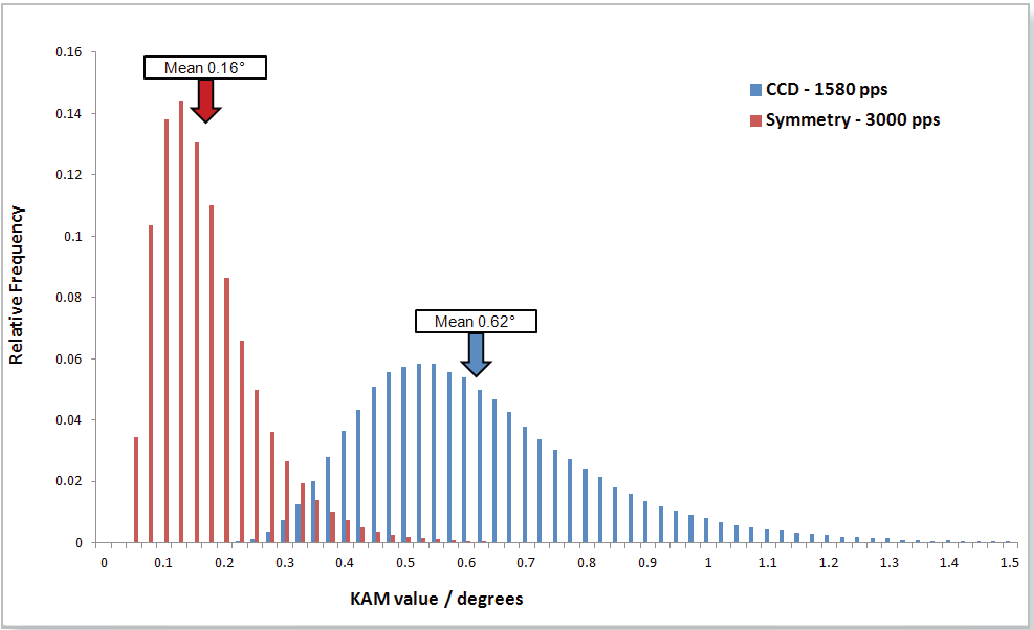
Fig. 4 — Comparison between the KAM distributions in the maps presented in Fig. 3.
The benefit of this improvement in angular precision would be greatest when studying small changes in orientation (such as across dislocation arrays), when studying boundary properties (especially misorientation rotation axes) or when using EBSD data to calculate geometrically necessary dislocation densities.
In the second example the Symmetry detector has been used to analyse a duplex stainless steel that had been rolled and subsequently heat treated, causing the formation of Chi and Sigma intermetallic phases. In this case the detector resolution was set at 622 x 512 pixels, and the acquisition speed was 493 pps with a 99.7% hit rate. The phase map of the analysis area is shown in Fig. 5a, and in Fig. 5b a grain relative orientation distribution (GROD) map is plotted for the austenite phase. In a GROD map, every pixel in each grain is coloured according to its disorientation from that grain's mean orientation, resulting in a map that highlights areas of deformation within the sample. The map shows local areas of orientation change close to boundaries and associated with surface scratches, but also highlights regions of deformation at triple junctions associated with the intermetallic phases. A transect across one grain and towards a deformation zone is marked by the red line, and the orientation change along this transect is shown in Fig. 5c. It is clear that the angular precision of these data is significantly under 0.1°, allowing orientation changes as small as 0.05° to be resolved, yet at acquisition speeds usually associated with heavily binned EBSPs.
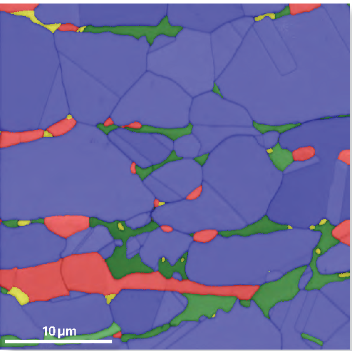
Fig. 5a — Phase map of a heat-treated duplex steel. 622 x 512 pixel resolution patterns were collected at 493 pps. Blue – austenite, Red – ferrite, Green – Sigma, Yellow – Chi.
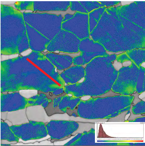
Fig. 5b — Grain relative orientation distribution map of the same area. Colour scale ranges from 0 to 1°. Red line marks transect shown in Fig. 5c.
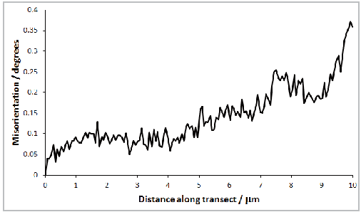
Fig. 5c — Misorientation profile along the transect in Fig. 5b, relative to the starting point.
Conclusion
This technical bulletin has highlighted one of the most dramatic advantages of using the CMOS-based Symmetry detector compared to traditional CCD-based detectors. Even at unprecedented acquisition speeds, Symmetry can collect diffraction patterns with high pixel resolution patterns, enabling improvements in hit rate, phase discrimination and angular resolution. The examples shown here prove that boundaries as low as 0.5° can be effectively measured at speeds in excess of 3000 pps, while higher resolution patterns at speeds around 500 pps enable the resolution of orientation changes as low as 0.05°.
Symmetry: the EBSD detector without compromise.

