Products
FIB-SEM
Nanomanipulators
OmniProbeOmniProbe CryoSoftware
AZtec3DAZtecFeatureAZtec LayerProbeTEM
Hardware
EDSUltim MaxXploreImaging
TEM CamerasSoftware
AZtecTEM
 Part of the Oxford Instruments Group
17th November 2021 | Author: Dr Haithem Mansour
Understanding the microstructure of materials is necessary to improve their performance and mechanical properties and even the smallest feature could be critical. For example, Funakawa et al. [1] showed in 2013 that controlling nanometre-sized carbides and dispersing them into ferrite grains has achieved an important improvement in mechanical properties of steel.
For many years, the conventional instrument to evaluate these fine structures was the transmission electron microscope (TEM), but nowadays it is possible to do similar analyses in scanning electron microscopes (SEM). This became possible thanks to:
There is tremendous interest in achieving TEM-like analysis in the SEM, because it has many advantages:
The identification of precipitates in steel and alloys typically requires the analysis of characteristic X-rays and electron diffraction. In this blog, I will focus on the Energy Dispersive X-ray Spectroscopy (EDS) technique.
1. Sample preparation
Sample preparation is a crucial step that will determine if analysis will be possible and will have an impact on the quality and accuracy of the results. Many polishing techniques can be used on steel and alloys, for example: mechanical polishing, ion milling and electropolishing.
For steel and alloys samples, mechanical polishing is the most used. It usually consists of several steps of polishing to remove damaged surface material and to achieve the best possible finish. The polishing recipe (including size of abrasive particles, time of polishing, use of oxide or diamond particles) is often different from one material to another.
2. Plasma cleaning
To achieve optimum results, the sample doesn’t only need to be well prepared but also clean. Sample preparation and handling introduce hydrocarbon contamination that forms a layer on top of the surface when it is irradiated by the electron beam. This phenomenon is accentuated at low kV which makes it a problem for nanoanalysis.
Plasma cleaning in SEM, typically using Oxygen plasma, has proven to be highly effective in removing hydrocarbon contamination. As you can see in the figure below, the plasma cleaning did a very good job in removing most of the contamination on the surface.
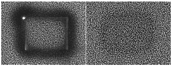
Fig. 1. (Left) Contamination build up after scanning an area; (Right) Almost complete suppression of contamination using Plasma cleaning [2]
3. Observation parameters and appropriate detector selection
SEM experimental conditions are crucial to obtaining high spatial resolution. X-ray interaction volume decreases with the acceleration voltage, which means analysing nano-features (<100nm) with EDS requires working at low accelerating voltages (<5kV) when analysing bulk samples. In addition, low beam current and short working distance (WD) are required to minimise the size of the electron probe and maximise signal. To work under those extreme conditions for EDS, a high resolution FEG-SEM is needed, and this typically means the need for beam deceleration mode to achieve the smallest beam spot and very little beam convergence. In-lens or in-column detectors will be very useful as well with such experimental conditions.
These operational conditions are the opposite conditions required for conventional EDS, hence the need for a dedicated solution. The Ultim Extreme EDS detector was developed and optimised for ultra-high resolution low kV analysis. Its windowless compact design makes it ideal for working with the extreme conditions explained above.
4. Drift correction
Analysing nano-features will require scanning the same area at very high magnification (>50k X) for several minutes and, depending on the stability of the SEM (temperature, cooling, vibration, contamination…etc), the scanned area could shift during the analysis. Correcting this shift is crucial to achieve a good result by the end of the analysis. To overcome this issue, the AZtecLive software provides very effective drift correction routines (AutoLockTM) which are essential when working at the nanometre scale.
Examples of high spatial resolution SEM-EDS for the study of steels
The first example, from JFE steel, is a study of precipitates in steel. The figure below shows the same area scanned at two different acceleration voltages, first at 15kV and then at 1.5kV. We can see the improvement in resolution, and in particular surface sensitivity, in both the electron image and the EDS map, which reveals the existence of MnOB nano precipitates.
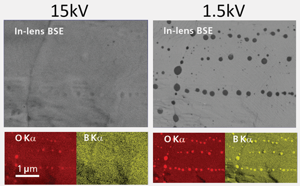
Fig. 2. (Left) EDS map acquired at 15kV (Right) the same area acquired at 1.5kV reveals the existence of MnOB precipitates. (Data courtesy of JFE Steel)
The second example is a collaboration with the University of Manchester and is a study of an oxide-filled crack in a metallographic sample, polished down to 1 µm diamond finish. The figure below shows the EDS analysis of the same area at 15kV using a 150mm2 conventional EDS and 1.5kV using a windowless Extreme detector. The details revealed in the Fe maps acquired at 1.5kV clearly show the presence of a thin 2-layer oxide structure: an Fe-poor oxide adjacent to the oxide/metal interface. These details are absent in the 15kV map.
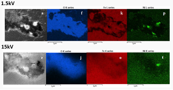
Fig. 3. SE images observed with primary electron beam energy of 1.5kV (a) and 15 kV (e). EDS maps collected at 1.5kV : O K (f), Fe L (k), Ni L (p) and EDS maps collected at 15kV: O K (j), Fe K (o), Ni K (t).
We hope these examples show how by using the right equipment and workflow you can achieve high resolution TEM-like analyses in SEM. If you would like to learn more about high resolution techniques in SEM, read this blog about TKD or watch this tutorial about STEM-SEM.
[1] Y. Funakawa, T. Fujita and K. Yamada: JFE Giho 30 (2012) 15.
[2] “Application of Plasma cleaning technology in Microscopy”, XEI Scientific, Tom Levesque and Jezz Leckenby
We send out monthly newsletters keeping you up to date with our latest developments such as webinars, new application notes and product updates.
© Oxford Instruments 2024