LayerProbe Brochure
This 8 page brochure shows the features, benefits and operating principles of LayerProbe - and the many applications it is applied to.
 Part of the Oxford Instruments Group

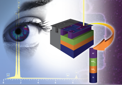
LayerProbe is an exciting software tool for thin film analysis in the SEM. An option for the AZtec EDS microanalysis system, LayerProbe is faster, more cost-effective and higher resolution than dedicated thin film measurement tools.
Thin film analysis in the SEM
Characterises multiple layers beneath surface of the specimen
Non-destructive analysis
Thickness and composition of multiple layers from 2 nm to 2000 nm
Lateral resolution down to 200 nm
Easy to set-up for routine user, and a cost effective extension of your SEM or FIB-SEM
An extension to AZtecLive: seamlessly integrated and easily retrofittable to existing installations
LayerProbe analyses the composition and thickness of the surface and sub-surface layers of a specimen. A non-destructive tool based on established microanalysis technology, it is more cost-effective, higher resolution, and more accurate than dedicated film measurement tools.
LayerProbe complements the elemental and phase information gained from conventional EDS analysis by also calculating the composition and thickness of the individual layers beneath the surface.
This 8 page brochure shows the features, benefits and operating principles of LayerProbe - and the many applications it is applied to.
Here we present a new technique that enables measurement of the local thickness and composition of TEM lamellae and discuss its application to the failure analysis of semiconductor devices.
In this webinar, we discuss how the software solution AZtec LayerProbe uses EDS to measure the compositions and thickness of thin layers and how you can achieve successful results, including for TEM lamella.
Photovoltaic (PV) cells are an attractive option for generating low carbon renewable energy but traditional designs often include undesirable toxic compounds and must be manufactured under special conditions.
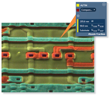
LayerProbe is ideal for a wide range of applications, including back- and front-end chip manufacturing, semiconductor R&D, optical and industrial coatings, nanoelectronic devices...
LayerProbe provides a new way to quantify TEM lamella thickness and quality in situ - as well as a complimentary technique to the cross-sectional analysis of layered specimens on FIB-SEMs.
LayerProbe is based on proven technology and has significant benefits compared to alternative techniques
A comparison of LayerProbe with other techniques
| LayerProbe | Ellipsometry | FIB/TEM | RBS | |
| Non-destructive | Yes | Yes | No | Yes |
| High spatial resolution | Yes | No (>>1 micron) | Yes | Yes |
| Rapid analysis | Yes (each point takes seconds) | Yes | No (several hours) | No |
| Cost | Relatively inexpensive | Expensive | Very expensive | Extremely expensive |
How accurate is LayerProbe?
Comparison of ALD layers on silicon substrate
| LayerProbe Thickness (nm) | Density (gcm-3) | Ellipsometry Thickness (nm) | Refractive Index | |
| HfO2 | 28.1 ± 0.1 | 9.4 | 33.6 ± 5 | 2.04 |
| Al2O3 | 57.0 ± 0.2 | 3.0 | 52.8 ± 5 | 1.64 |
LayerProbe EDS and RBSD composition measurement
| LayerProbe - Stoichiometric Ratio | RBS - Stoichiometric Ratio | |
| Hf /O | 2.13 | 2.07 |
| Al /O | 1.56 | 1.60 |
Example: PCB Application - Au on Ni on Si substrate
LayerProbe and XRF thickness measurement
| LayerProbe Thickness (nm) | Density (gcm-3) | XRF Thickness (nm) | |
| AU | 60.1 ± 0.7 | 19.3 | 61 ± 25 |
| Ni | 123.5 ± 0.7 | 8.9 | 141 ± 24 |
SEM cross section measurement confirms the result...

© Oxford Instruments 2026
