✔️ Ultimate performance
The only windowless EDS detector with excellent low energy performance, resolution guaranteed at CK of 46 eV or better at all count rates up to 50,000 cps.
 Part of the Oxford Instruments Group

Ultim Extreme ∞ (“Infinity”) is a breakthrough solution for ultra-high resolution FEG-SEM. This unique detector enables EDS data collection at very low kV (e.g. 1-3 kV) and very short working distance to provide elemental analysis under the conditions required to analyse nanomaterials and surfaces at the highest SEM resolution. The maximum sensitivity guaranteed due to specific technological solutions such as: specially shaped sensor, windowless design, proximity of sensor to the sample, small electron trap and very high solid angle.
View Brochure Request Pricing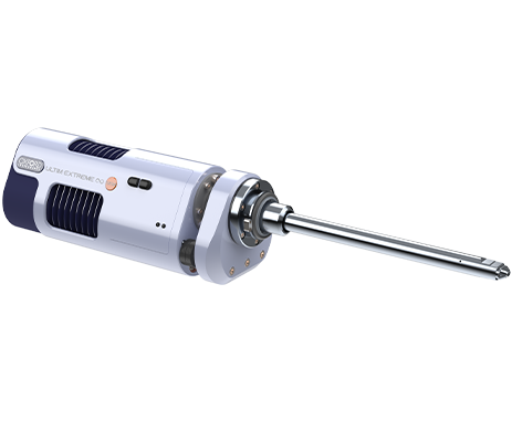
Ultim Extreme Infinity delivers solutions beyond conventional micro and nano-analysis:
The only windowless EDS detector with excellent low energy performance, resolution guaranteed at CK of 46 eV or better at all count rates up to 50,000 cps.
Excellent low energy spectral resolution is particularly important when analysing samples using very low kV. Processing the data with TruMap can deconvolute SL/NbM and MoM overlaps.
New capabilities when trying to solve the most difficult overlaps or to display trace element information.
The significant increase in the light element signal allows fast collection, and real-time data processing.
Mapping of small, low intensity features at the imaging conditions needed to see the structures.
Extreme Infinity measurement allows new levels of detectability for elements such as nitrogen.
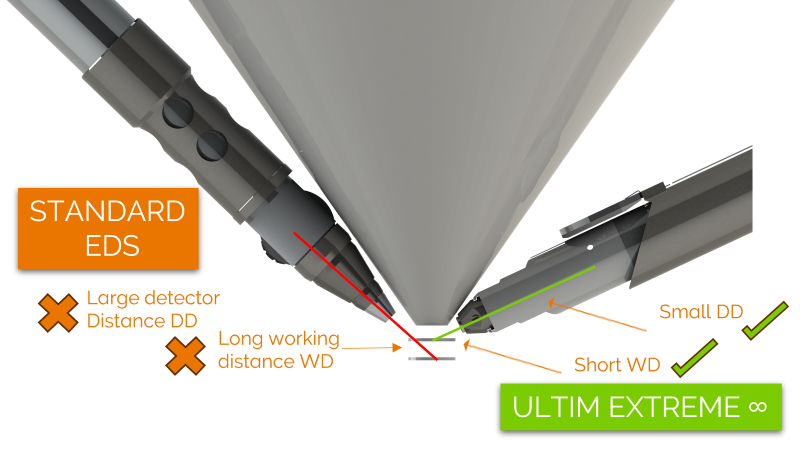
< 3 kV, even down to 1 kV, low current (100 s pA), short WD (<5 mm, In-lens detectors for imaging).
Fast collection, real-time data processing from a bulk sample & significant signal increase from small features/low concentration phases.
Sub – 10nm element characterisation in the FEG-SEM.
New levels of detectability for elements such as nitrogen and oxygen.
Characterise surfaces in the SEM, down to 1 kV materials characterisation & move away from TEM, or surface science tools.
Analyse materials where beam sensitivity limits accuracy and usefulness of EDS (biological, polymers).
*Requires sample material that exhibits electron induced X-ray emission of LiK
Working at low accelerating voltage (kV)/ short working distance (WD)
To achieve nanometre spatial resolution on the SEM, it is necessary to use low accelerating voltage and low beam current which are ideal imaging conditions. However, that also means that the X-ray data has to be collected at the exact set of conditions. At these conditions interaction volume is small, X-ray intensity is low and another challenge is that only a few X-ray lines are being excited.
These requirements are beyond conventional EDS capability. In order to see the smallest structure on the sample, there is a big sacrifice in the amount of X-ray signal being generated. X-ray count rates from very small structures are always very low and in that part of the spectrum where X-ray peaks are complex and very close together.
Some of the main challenges of X-ray analysis at imaging conditions compared to conventional 10kV -20kV analysis are following:

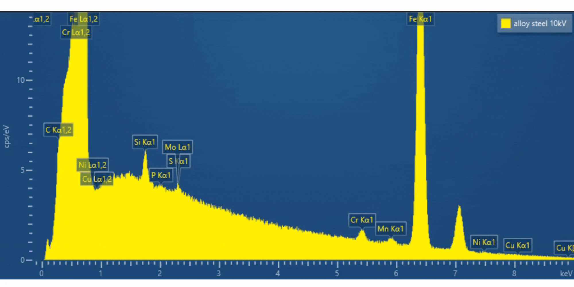
Interpreting low-energy X-ray data can be complex due to the closely spaced and low-intensity X-ray peaks. As a result, accurately interpreting the spectral information such as spectral overlaps and automated identification requires the highest possible spectral resolution. When analysing the low-energy portion of the spectrum, the resolution of the carbon peak (CK) is particularly important, while the manganese K (MnK) line may not even be present.
C resolution: showing importance of high energy resolution is particularly important in the low energy part of the spectrum. Higher energy resolution will result in peaks being sharper and at the correct position (no shift).
When only comparing better spectral resolution on pure standard sample (eg BN) we notice sharper peaks, but the real difference is displayed when analysing a sample. An example of different resolution can be seen in the below video, showing collected spectra. The video demonstrates how with the poor energy resolution (>60eV) S L, N K, Nb M peaks are not distinguished from the background, also Cr L line cannot be separated from the O K. However, if the detector has excellent energy resolution (<46eV) then it is possible to resolves these problematic overlaps and low intensity signals
Excellent low energy resolution means excellent characterisation at high spatial resolution. Correct display of elemental distribution requires high spectral resolution performance. While some information displayed is similar with lower (>60 eV) and higher resolution (<46 eV) without spectrum processing (integral map), nevertheless, in some phases the concentrations are clearly different. Processing the data with TruMap can sort out S L/Nb M and Mo M overlaps for accurate display of element variation only if the detector low energy resolution is high enough (<46eV).
.gif)
Tru-Q™ technology revolutionised EDS when introduced with AZtec Energy all the way back in 2011. Using a fundamental EDS detector calibration measured with a synchrotron, enabled accurate characterisation of each detector type on a SEM. This characterisation Tru-Q powered EDS to reach new levels of accuracy and reliability in quantitative analysis, AutoID, peak deconvolution and real-time map correction.
Find out how Tru-Q revolutionised standardless quantitative analysis by watching our webinar: Quantitative EDS Explained: How to achieve great results
Tru-Q IQ takes things to the next level where each and every Ultim Max Infinity detector is characterised on a SEM during manufacture and then given its own unique detector optimisation. This optimisation is then confirmed during installation on your SEM. This gives unparalleled performance with every Infinity detector able to characterise accurately the most complex analysis challenges, solve challenging low energy peak overlaps and find smaller concentrations of elements.

The perfect fit to the spectrum data provided by Tru-Q IQ means minor elements like phosphorus can be identified under a complex overlap of NbL and MoL lines.
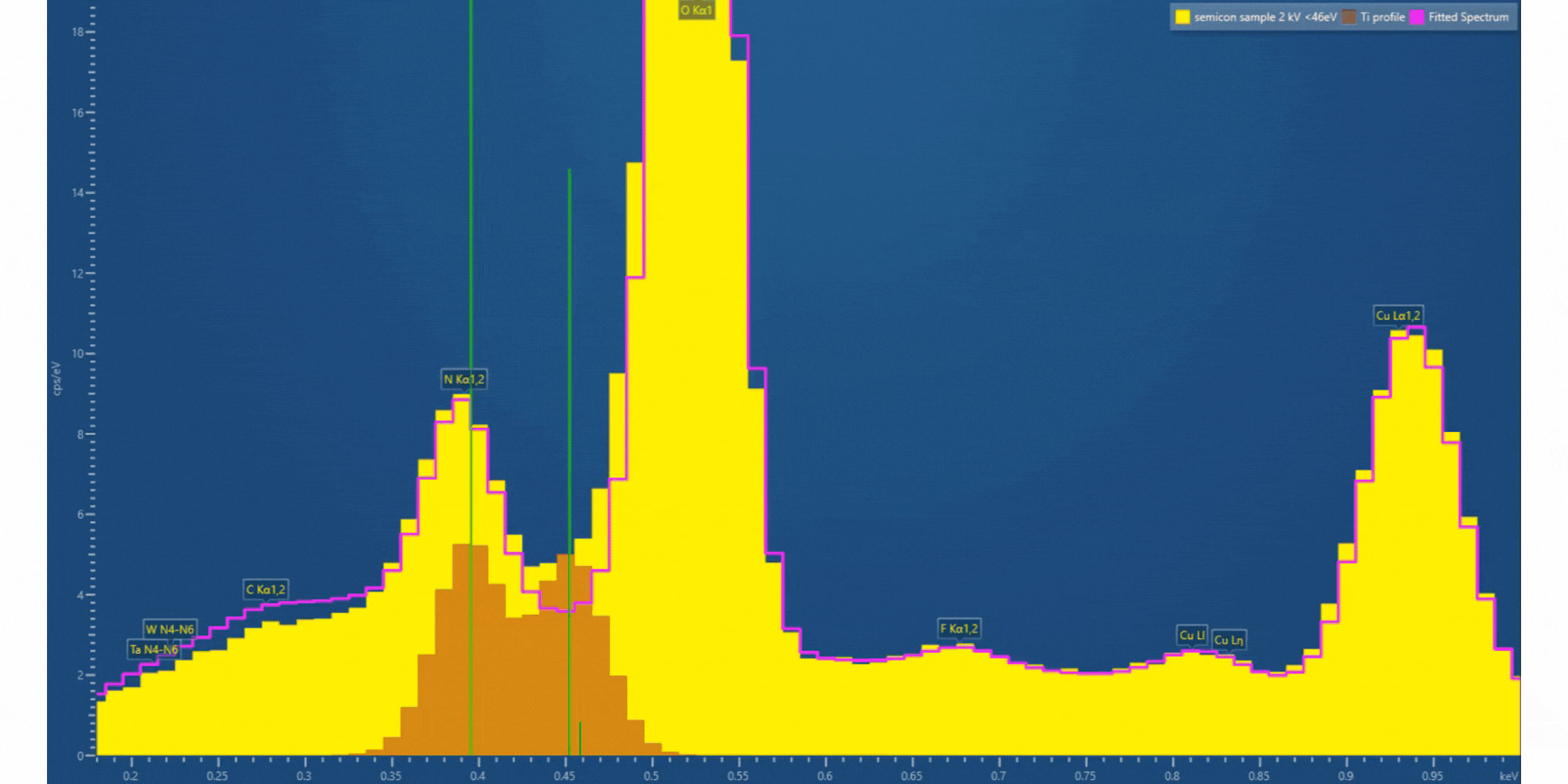
The most difficult analytical challenges require Tru-Q IQ. This next example shows semiconductor analysis at low kV conditions. When analysing this sample with nano-metre size structures the signal from Ti is weak. Without individual detector optimisation, Ti is not recognised by autoID due to the low signal and also the overlap with NK. With individual detector characterisation and optimisation, even when analysing low intensity and overlapping peaks, such as TiL, autoID will identify the presence of this element and the correct conclusion about the existence of the TiN layer can be drawn.
Detector resolution is not the only parameter. Improved results can be achieved after individual detector characterisation and optimisation-unique new Tru-Q IQ. TruMap can sort out SiL/CrL/OK/MoM overlaps for accurate X-ray maps if the detector low energy resolution is high enough. However, we can achieve even better results because after detector optimisation, improved low energy lines fitting is achieved, which gives higher auto ID confidence and consequently better display of elemental distribution. By characterising the detector and optimising the detector fitting, changes in peak shape and position are corrected. Here we see that, without detector optimisation the Mo signal is lost and the Nb/Mo overlap is not completely deconvoluted.
.gif)

The Ultim Max Infinity EDS detector unlock the infinite potential of EDS for characterising materials in the SEM. They combine unparalleled accuracy, sensitivity and speed to power AZtec Live software to solve more complex analysis challenges. It provides the ultimate solution for nano-characterisation and light element detection, most accurate analysis and high count rate mapping of micro-structures.

The Xplore EDS detector is designed for routine analysis in the SEM. It contains the same proven technology from the class leading UltimMax high large area detectors, so users can expect the same high-quality results, but in a much smaller package. The Xplore complements our comprehensive EDS portfolio and means that AZtecLive real-time chemical imaging is now available to all users.
Find out more
Unity is a new detector for a revolutionary new imaging technique in the Scanning Electron Microscope (SEM). Unity is the world’s first Backscattered Electron and X-ray (BEX) Imaging detector. It seamlessly combines backscattered electron and X-ray signals to deliver rapid high-definition colour images embedded with elemental data as you navigate around your sample.
Find out more
© Oxford Instruments 2026
 Powered by Bioz