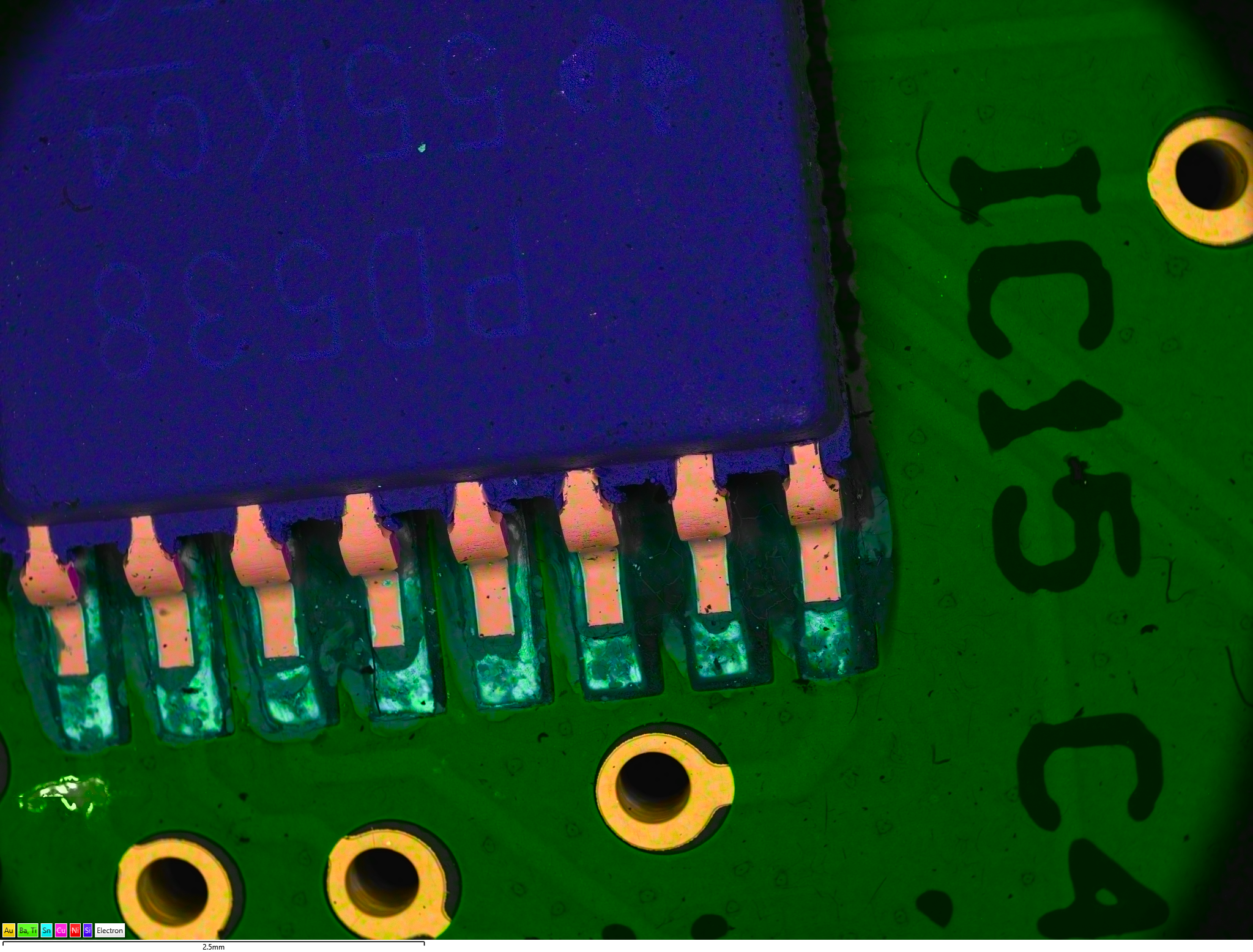
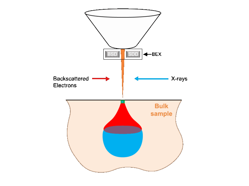
Part of the Oxford Instruments Group
Expand

What is BEX?

Backscattered Electron and X-ray (BEX) imaging is a technique for Scanning Electron Microscopy (SEM) which acquires data simultaneously from both Backscattered Electron (BSE) sensors and X-ray sensors, such as silicon drift detectors, all located within the same sensor package.  

The combined signals produce high resolution colour images containing topographic, crystallographic, and compositional information which can be acquired with the low dwell times of an imaging system all while operating at ‘standard’ SEM imaging conditions.

Ask a question

Examples of BEX Imaging

Ti
Ni
Al
BEX map of whole 12 mm diameter sample stub. 20 kV, 2 nA, image acquired in 30 mins
High resolution BEX image of electronic chip. 20 kV, 1.5 nA, 2K image acquired in 10 seconds

Imaging Technologies in SEM

Imaging with Secondary Electrons 

Historically, the most common modality is Secondary Electron (SE) imaging, which involves the detection of low energy electrons (~50 eV) that are ejected from the sample due to inelastic interactions between the primary beam and sample surface. The electrons are detected by an Everhart-Thornley detector consisting of a positively biased Faraday cage, scintillator, and photomultiplier.

The signal generated originates from very close to the sample surface and as the angle of incidence of the primary beam moves away from normal the number of electrons that escape the bulk material increases, this means the SE imaging contains information about local sample topography.

Secondary Electrons (green) are generated near the sample surface and produce a greyscale image containing information about sample topography.  20 kV, 1 nA, 15 seconds to acquired. 

Imaging with Backscattered Electrons

Backscattered Electron (BSE) imaging involves the detection of electrons originating from deeper within the sample. The BSE electrons are higher energy, since they result from elastic interactions between primary beam and sample which change the trajectory of the incident electrons such that they are scattered back from the sample surface. An SE detector is ineffective at measuring these electrons since its remote position from the sample results in very low signal. Instead a BSE detector will typically consist of p-n semiconductors arranged immediately below the SEM objective lens to maximise signal collection.

The scattering interactions which generate the BSE signal are much stronger in samples made of heavier elements. Consequently, a BSE image contains information about sample composition where heavier phases appear brighter. While simple operation of BSE detectors shows atomic number contrast if the sensors are arranged into two or more segments, the signals from each sensor can be combined to show topographical information.

Backscattered Electrons (red) are generated from below the sample surface and produce a greyscale image containing information about sample composition. 20 kV, 1 nA, 15 seconds to acquired.

Imaging with BEX

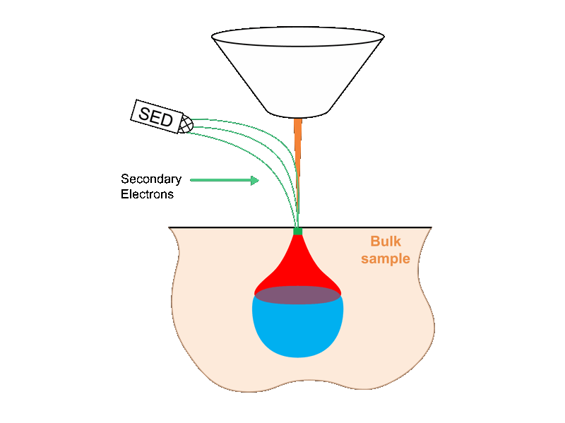
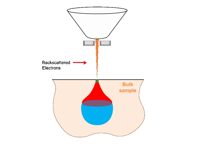
BEX combines BSE sensors with X-ray sensors which are placed in the same geometry as a standard BSE detector, immediately below the objective lens. The X-ray sensors, typically silicon drift detectors (SDDs), measure characteristic X-ray emissions generated as the sample is irradiated by the SEM electron beam in the same manner as an EDS detector. Software algorithms process the collected X-ray signal to automatically identify which elements are present. These elements are then assigned colours which are layered along with the signal from the BSE detector to provide a final image.

When compared to SE or BSE imaging a BEX imaging system provides more information about sample composition and elemental distribution in the same acquisition time, with the same operating conditions.

In contrast to an EDS detector, a BEX imaging system has sensors with an incredibly high solid angle. This ensures X-ray information can be collected at normal imaging speeds and with typical imaging beam currents (~1 nA). The position of the SDD, near the objective lens, also eliminates shadowing effects from sample topography and allows for sample investigation at a wider range of working distances.

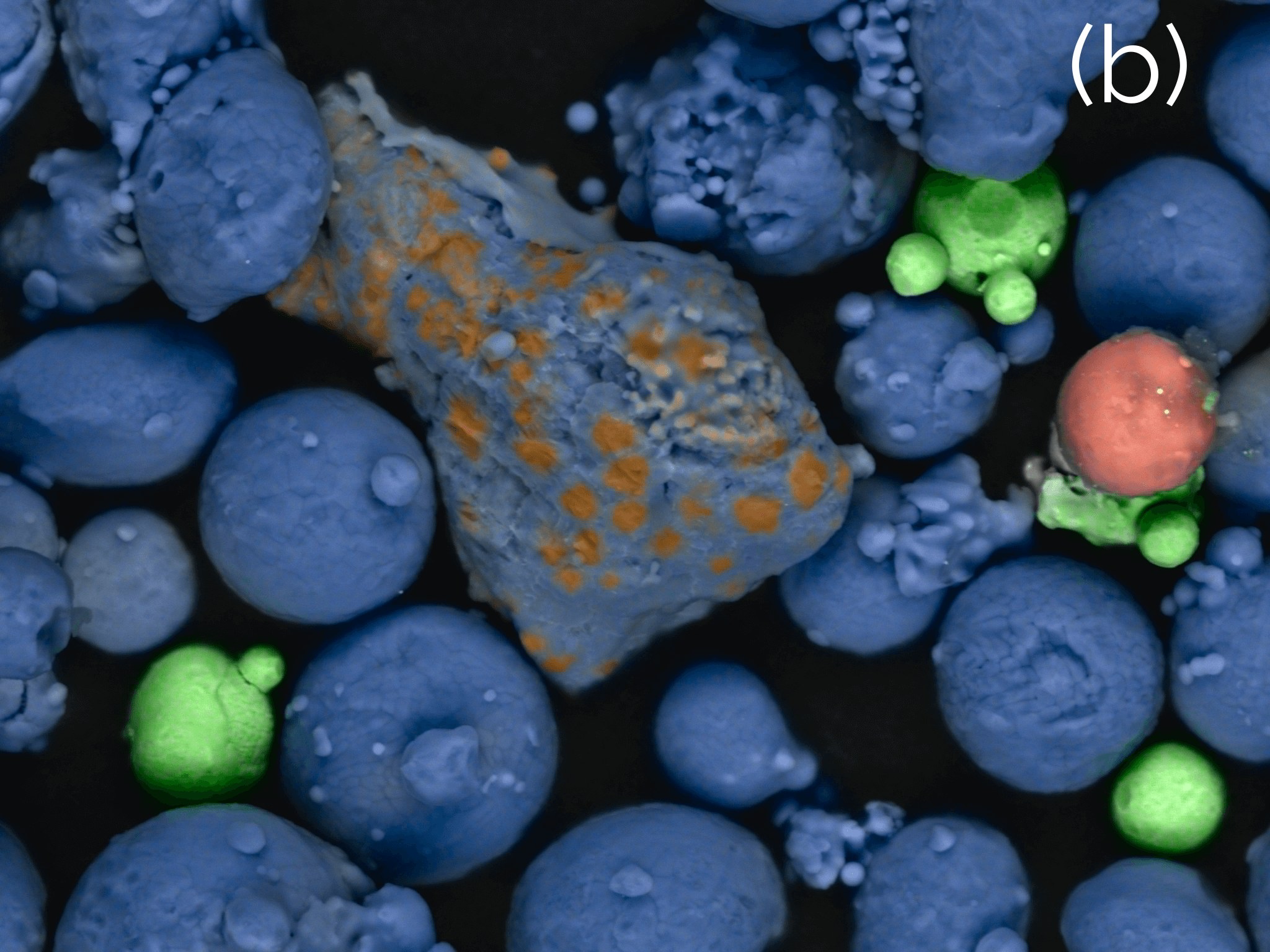
BEX coloured electron image
Backscattered electron image
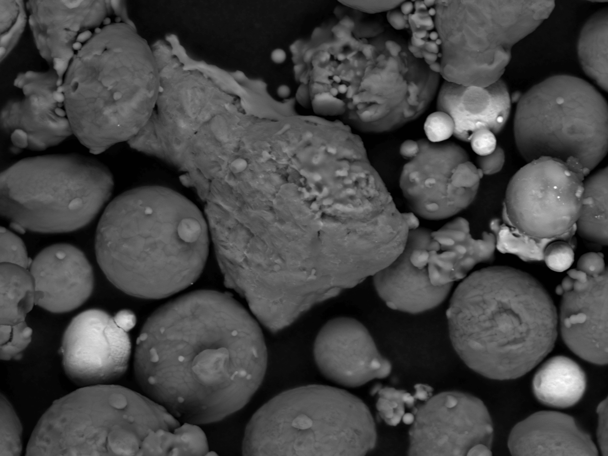
Backscattered Electrons (red in a.) and X-rays (blue in a.) are detected and combined to produce a BEX colour image showing sample composition b). 20 kV, 1 nA, 15 seconds to acquired.

Discover how to get more from BEX...