AZtecHKL
This 16 page brochure illustrates why AZtec is the leading EBSD analysis platform on the market. Covers both hardware and software.
 Part of the Oxford Instruments Group

The most powerful EBSD software available, AZtecHKL combines speed and accuracy of results for routine analysis, with the flexibility and power required for applications that push the frontiers of EBSD.
Unleashes the potential of the world's most sensitive CMOS-based EBSD detector, Symmetry S3
Optimised for nanoscale orientation mapping using Transmission Kikuchi Diffraction (TKD)
AZtec couples Oxford Instruments’ understanding of real customer needs for routine EBSD analysis, with the flexibility and power required for applications that push the frontiers of EBSD.
Developed by the market leader with global customer support and over 40 years experience in nanoanalysis, AZtec meets the ever more challenging requirements of analysis at the nanoscale.
Fast and powerful
Easy to use
Flexible
Innovative
This 16 page brochure illustrates why AZtec is the leading EBSD analysis platform on the market. Covers both hardware and software.
EBSD Explained is a 24 page tutorial that not only gives newcomers a solid foundation in the underlining science of the subject, but also shows how the theory is applied in practice to get reliable and accurate EBSD results.
Symmetry S3 is a 3rd generation detector based on the advanced CMOS technology and unique design features that have made Symmetry the market’s leading EBSD detector.
Reconstructing the metamorphic evolution of rocks often depends on the identification of key minerals that are only stable at specific temperatures and pressures. Combined EBSD and EDS analyses enable more rigorous phase identification than conventional techniques, with the added benefit of providing insights into a rock’s deformation and chemical history.
Approx View time: 7 minutes
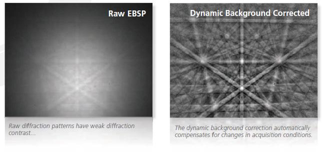
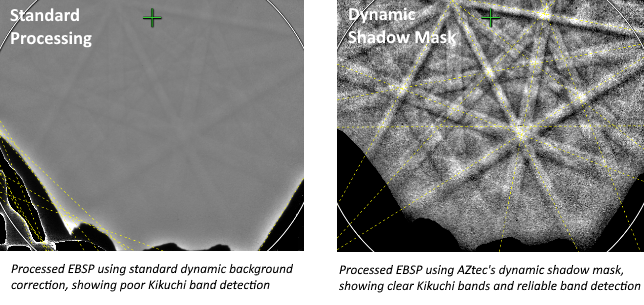
AZtec implements an intelligent band detection routine that determines which of the detected bands should be used in the indexing.
In some applications, high magnetic fields from the SEM lenses distort the electron backscattered diffraction patterns. This distortion curves the Kikuchi bands and shifts the pattern centre but can be corrected automatically using AZtec.

The EBSD indexing routine is critical in achieving accurate results - AZtec uses a new method, Class Indexing.
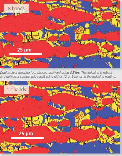
AZtec correctly identifies phases with similar crystal structures by comparing bandwidth.

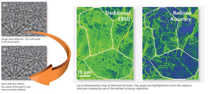
Refined Accuracy Algorithm
A new and innovative ‘Refined Accuracy Algorithm*’extends traditional EBSD analysis to deliver unrivalled accuracy and level of detail...
AZtec Refined Accuracy delivers:

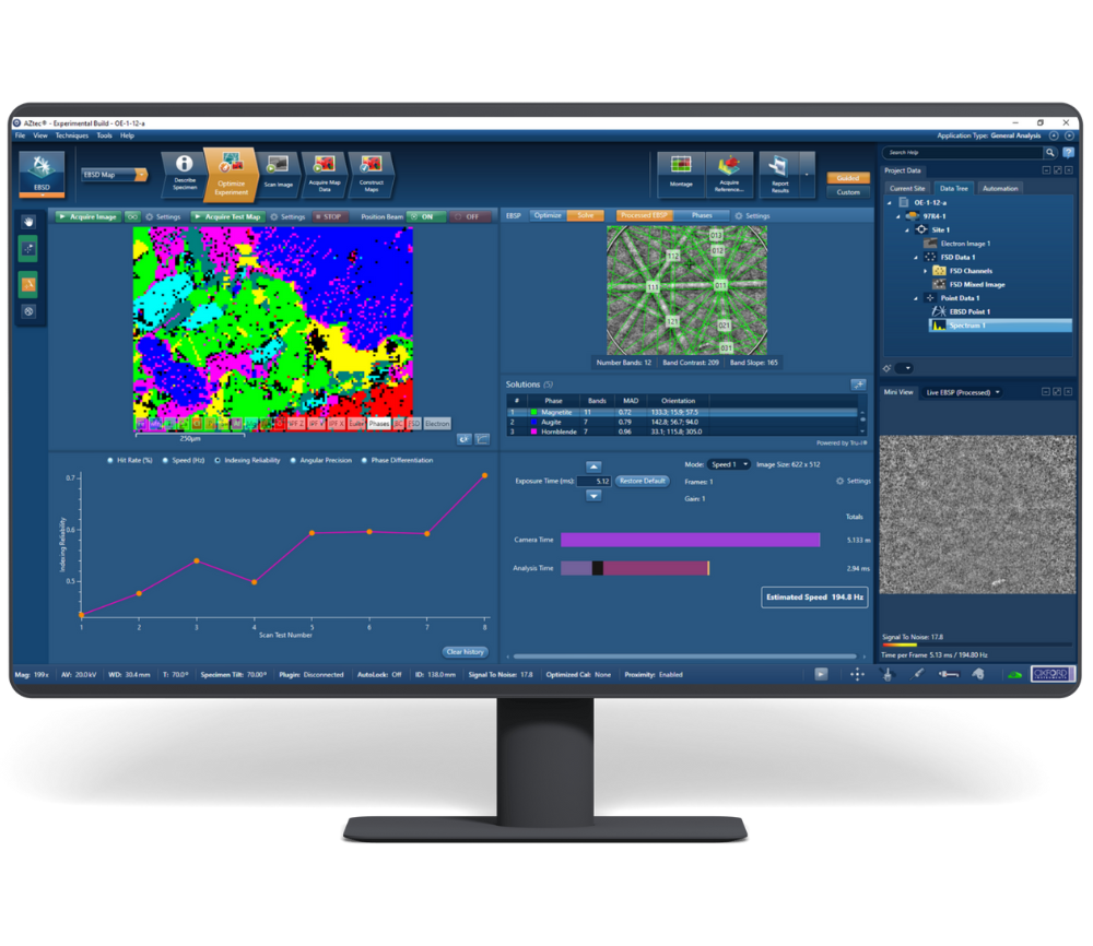
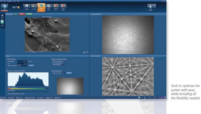
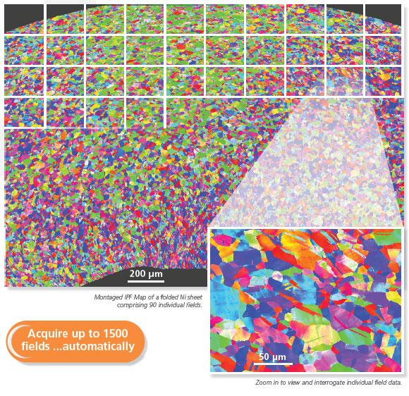
Optimising the system for data acquisition is easier and more automated than ever before
AutoLock

All AZtec acquired images can be used for specimen navigation and relocation at a later date - even on a different microscope.

The CMOS detectors can incorporate up to 5 forescatter detector diodes
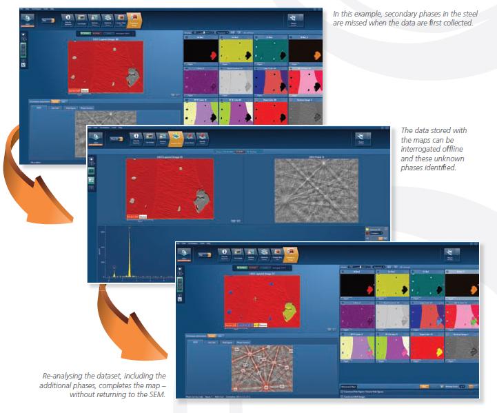
AZtecHKL re-analysis is completely flexible:

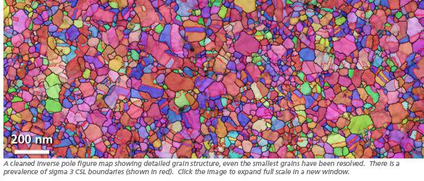
Despite significant technological developments in recent years, the conventional EBSD technique is still limited by the pattern source volume to resolutions in the order of 25-100 nm. This is insufficient to measure accurately truly nanostructured materials (with mean grain sizes below 100 nm).
A new approach to SEM-based diffraction has emerged. This uses an electron-transparent sample coupled with conventional EBSD hardware and software. This technique referred to as transmission EBSD (t-EBSD: Keller and Geiss, 2012) or SEM Transmission Kikuchi Diffraction (TKD: Trimby, 2012) has been proven to enable spatial resolutions better than 10nm.
TKD in AZtec
AZtecHKL includes a dedicated TKD navigator that, coupled with the exceptional sensitivity of our CMOS detector range, always delivers high quality TKD results. There are a number of unique TKD-focused innovations, enabling an instantaneous switch from conventional EBSD analyses to TKD:

© Oxford Instruments 2026