Products
FIB-SEM
Nanomanipulators
OmniProbeOmniProbe CryoSoftware
AZtec3DAZtecFeatureAZtec LayerProbeTEM
Hardware
EDSUltim MaxXplore for TEMImaging
TEM CamerasSoftware
AZtecTEM
AZtecWave combines the high spectral resolution of the Wave Spectrometer, to resolve X-ray peaks and quantify minor and trace elements, with the speed and flexibility of EDS. This delivers an advanced and complete solution for compositional analysis on the SEM.
EDS and WDS are fully integrated and combined in the AZtecWave software, facilitating major element acquisition with fast and accurate EDS (powered by Tru-Q®) and enabling WDS to be effectively utilized when EDS reaches its limitations:
For the detection and accurate quantification of trace elements (<1000 ppm)
For the separation of X-ray peak overlaps, bringing certainty to element identification and accuracy to quantification
By bringing together the benefits of both EDS and WDS – speed and sensitivity – AZtecWave provides accurate answers, fast. Solving real microanalysis challenges in the fields of metallurgy, geology, electronics, ceramics, semiconductors, batteries and many others.
Figure showing show AZtecWave automatically determines where to measure the WDS backgrounds to avoid peak interferences
AZtecWave brings electron microprobe (EPMA) like performance to the SEM – enabling an effective combination of highly accurate quantitative elemental analysis with high resolution electron imaging and other SEM-based techniques (e.g. EBSD).
| Composition of a stainless steel determined by a combination of EDS and WDS in AZtecWave
Quantitative X-Ray Analysis | ✔ |
Qualitative Spectrum Scanning | ✔ |
X-ray Mapping | ✔ |
Point Automation of WDS and EDS Acquisition | ✔ (Optional) |
WDS Standardisation | ✔ |
Guided Spectrometer Setup | ✔ |
Image Registration | ✔ (Option with upgrade) |
SEM Beam Stability Monitoring | ✔ |
Association of WDS and EDS | ✔ |
WDS Spectrum Simulation | ✔ |
Guided Sample Exchange | ✔ |
Guided Spectrometer Shutdown | ✔ |
Figure showing WDS scan positively identifying the presence of Co in a superalloy containing ~0.1 wt% Co, which is not apparent in the EDS spectrum
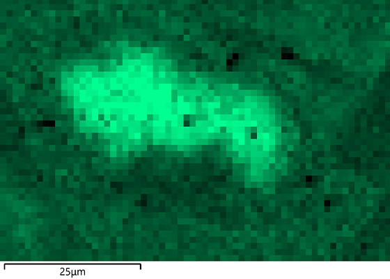
WDS element maps acquired from a babbitt alloy overlaid on a secondary electron image
Wavelength Dispersive Spectroscopy (WDS) lends itself to applications requiring quantitative compositional results from solid samples, particularly where concentrations of minor and trace elements need to be accurately determined. Application examples exist in a wide range of sectors, including metallurgy, geology, electronics, semiconductors, forensics, and energy generation and storage. Combining WDS with EDS analysis, through AZtecWave, provides a versatile system for non-destructive, compositional analysis in the SEM.
Discover detailed applications examplesThis tutorial explains the principles of Wavelength Dispersive Spectrometry (WDS / WDX) and how a WD spectrometer with Rowland Circle geometry works on an SEM in combination with EDS.
Watch this video & learn:
✅ The principles of Wavelength Dispersive Spectrometry
✅ How the Oxford Instruments Wave spectrometer works and how it enhances a SEM-EDS system
✅ When you might want to conduct WDS analysis and typical applications
This video presents how elemental mapping using a fully focussing Rowland circle, wavelength dispersive spectrometer (WDS / WDX) can enhance compositional mapping with Energy Dispersive Spectrometry (EDS / EDX), by enabling accurate mapping of elements present in trace concentrations or impacted by X-ray peak overlaps in the EDS spectrum.
This is illustrated with a WDS-EDS dataset collected from a steel sample containing multiphase inclusions, which was acquired using functionality that is coming soon to the AZtecWave software for combined WDS and EDS mapping.
WDS Scan is a new workflow in AZtecWave that enables the positive identification of elements affected by peak overlaps in the EDS spectrum, and/or present in trace concentrations (Less than 0.1 wt%).
Several different sample types will be presented as examples, including minerals, metals, and solder used in electronics. In addition, the tutorial will include demonstrations of how to; (1) acquire WDS scans using the different setup tools available, (2) identify the element lines present, and (3) compare multiple WDS scans and EDS spectra.
Discover how AZtecWave is the perfect solution to accurately and quickly detect all elements for challenging issues in the SEM. Discover how AZtecWave can help you achieve high quality results.
Discover the latest functionality for the AZtecWave WDS Scan, which powers the only WDS spectrometer with true electron-microprobe resolution and performance on the SEM. See how you can take data from SEM-EDS to a new level of certainty - by showing all peak overlaps fully resolved and accurately measuring all elements, including those present at the minor or trace level.
Both EDS and WDS are techniques that use X-rays, generated when an electron beam interacts with a material, to determine the elemental composition. Since EDS can collect all X-ray energies at the same time, compared to WDS which collects one X-ray energy (i.e., element-line) at a time, EDS is faster and therefore more commonly used for SEM-based compositional analysis. However, WDS does bring some significant advantages over EDS.
This tutorial will give a practical introduction to WDS and AZtecWave - our new software for combined SEM-based EDS-WDS analysis.
AztecWave accelerates your time to results, helping you achieve more in less time, with unparalleled accuracy and certainty. In this tutorial, discover how AZtecWave provides WDS detection and EDS speed with accuracy and accessibility.