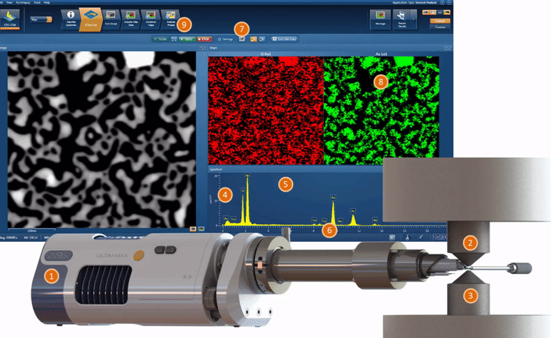
Ultim Max is the next generation of Silicon Drift Detectors (SDD) utilising our Extreme electronics to generate maximised sensitivity with increased throughput. This powers AZtecTEM, the market-leading software that delivers unparalleled elemental characterisation performance in the TEM.
Maximised sensitivity
Increased throughput
Stability at elevated temperatures
New drift correction methodology
Optimised for biological sample analysis
M2T quant for sample thickness measurements
Watch in situ chemistry changes as they happen with AZtecLive
These electronics were developed to detect Lithium by EDS in the SEM. Extreme electronics provides the lowest noise and processing available for SDD. They ensure excellent energy resolution and spectrum quality is achieved at all count rates. In the TEM very high count rates are difficult to achieve. However, the improved resolution at faster processing time (PT) achieved by extreme electronics allows you to use the counts you do generate more effectively and achieve the same results in potentially half the time.
An increase in both solid angle and take off angle combined with windowless detection and Extreme electronics has led to uncompromised x-ray sensitivity. This means that Ultim Max can now detect lower X-ray energies than ever before while maintaining exceptional sensitivity to conventional low energy X-rays such as oxygen and nitrogen.
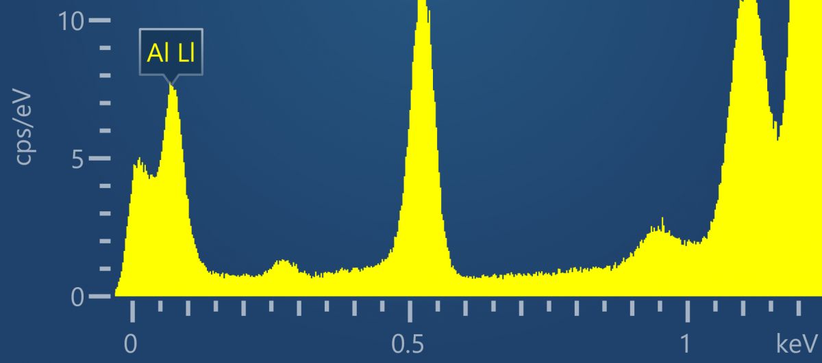
EDS spectrum of AlF collected at 200kV showing Al Ll x-ray line at 72eV.
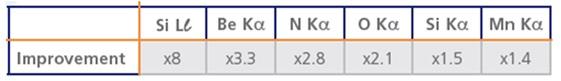
Ultim Max are windowless as standard. Windowless EDS detectors can be up to 8 times more sensitive than a conventional windowed EDS detector. For higher energy X-rays a conventional SDD is shadowed up to 40% by the window support while X-rays below 1 keV can be absorbed by the window material itself.
Improvement in sensitivity of a windowless detector vs. a conventional thin window detector for selected X-ray lines
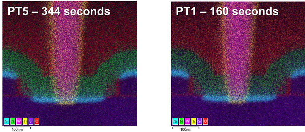
At high magnification, no matter how stable the microscope stage, drift correction is required to ensure that you continuously map the same area of a specimen. AutoLock is our robust drift correction algorithm that allows automatic drift correction at user-defined intervals. Autolock now supports frame-by-frame drift correction. Using the electron image collected simultaneously with every frame of an X-ray map, AutoLock can continuously correct for specimen drift. Using an image collected with the X-ray ensures continuous feedback so that users can manually adjust for any observed drift in the specimen z-direction. Not stopping an X-ray map to collect a drift correction image minimises the amount of electron dose a specimen receives. This ensures that spectrum images of even the most beam sensitive specimens can now be achieved.
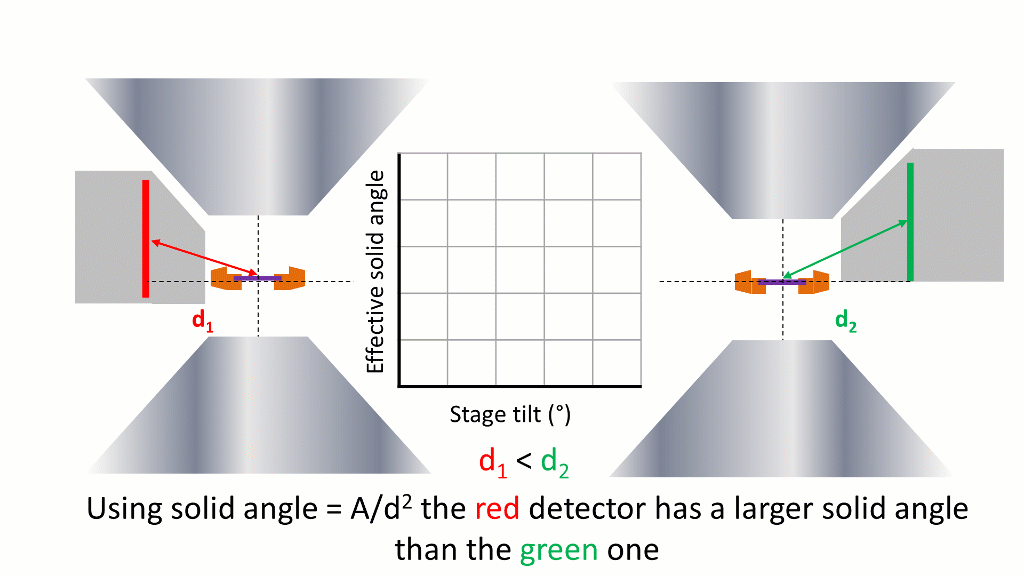
Solid angle is hugely important for TEM EDS applications to ensure you can collect as many of the counts that you generate as possible. In TEM EDS terms, the solid angle (Ω) is defined as the amount of the field of view from a point where an X-ray is generated that the active area of an SDD sensor covers.
In its simplest terms this is defined as:
(Ω) (sr) = A/d2
Where A is the active area of the SDD sensor and d is the distance it is located from the point an x-ray is generated.
For Ultim Max we have optimised the design of our large 80 mm2 and 100 mm2 active area SDDs. This allows the sensor to get as closer to the point in the specimen where the X-rays are generated. This maximises A and minimises d to give large solid angles up to 1.1 sr for a single detector, when calculated using the equation above.
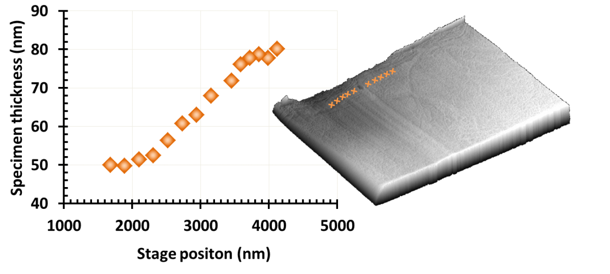
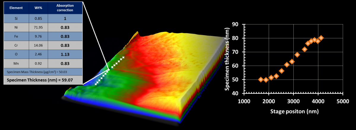
New quantification by mass thickness (M2T) reduces quantification inaccuracy from samples of varying thickness. TEM specimens are rarely uniform in thickness, and of particular importance, they are almost certainly not infinitely thin. This means that quantification using the well-known Cliff-Lorimer formulation can become inaccurate, especially if your specimen contains X-ray lines across a wide range of energies. This can be corrected for with thickness and density but these are difficult to measure.
With a single measurement on a sample supplied by Oxford Instruments, it is possible to calibrate for both the TEM beam current and the effective detector solid angle allowing for quantification in terms of mass thickness (ρt). AZtec then automatically applies the appropriate absorption correction to improve the accuracy of your quantification.
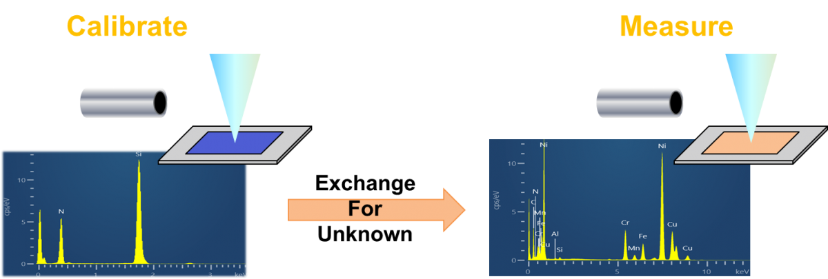
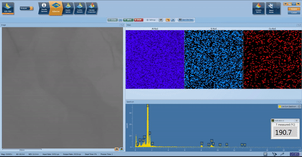
AZteclive, the revolutionary technology for EDS on the SEM now makes its way to TEM. Combining live electron images, live EDS maps and a continuously updating x-ray spectrum AZtecLive gives real-time, live, feedback of the elemental composition and morphology of a specimen. In TEM you are unlikely to achieve the count rates that allow you to elementally image a specimen as you navigate it. However, slow down the frame time to once every 2 or 3 seconds and you are now able to watch as the elemental composition of a specimen changes during in-situ experiments.
Screen capture of AZtecLive as an Au thin film is heated from 720°C to 800°C to observe elemental and morphological changes (sequence sped up 20x).
As important as solid angle is in a TEM it is important to ensure that the solid angle of your detector is usable. As no TEM specimen or holder is perfectly two dimensional an SDD detector can become shadowed at low specimen tilt reducing the effective solid angle. We design our EDS detectors to maximise the take-off angle. Due to the solid angle optimisation, the take-angle of Ultim Max and Xplore is larger than those of the equivalent X-Max detector. This means that there is less shadowing of the sensor at low tilt and therefore a larger effective solid angle. The result of this is more counts at lower tilt which is extremely important for specimens which require specific or low tilts such as semiconductor devices.
Observing reactions as they happen is now a crucial part of many TEM experiments. Collecting elemental information during these experiments have previously been difficult because EDS detectors are easily shadowed by bulky in situ holders and X-ray signals can become swamped by IR and visible radiation from the heater element. The improved take-off angle of Ultim Max and Xplore reduce shadowing of the SDD to collect more X-rays and allow mapping of samples in gas or liquid cells. Meanwhile, extreme electronics allow the detectors to keep collecting X-rays at higher specimen temperatures.
EDS spectrum of a 10 nm Au thin film collected at a specimen temperature of 900°C using Ultim Max TEM.
M2T quantification delivers results in terms of mass thickness (ρt) or in other words, the product to the specimen density and thickness. AZtecTEM allows users to input a density for a given specimen and by doing this the user is automatically presented with a measurement of the specimen thickness for each spectrum, without the need for EELS (Electron Energy Loss Spectroscopy) or complex diffraction techniques. Measuring local density is difficult and it may not be uniform, but for many samples, the average density can be estimated from the constituent elements and a very reasonable estimate of specimen thickness calculated. This allows users to understand more about their samples, especially when measuring parameters such as defect density which would now be possible to measure as a function of volume, not just area.
3D representation of 2D HAADF image and the associated measurements of specimen thickness using EDS
Ultim Max TLE, our flagship SDD detector for TEM. This detector is optimised to offer elemental characterisation at the atomic scale delivering maximum count rates at minimum probe sizes.
This performance is achieved using an optimised shape, 100 mm2 sensor, windowless construction, optimised mechanical design and extreme electronics.
Solid angle of 0.5 - 1.1 srad
Up to 8x increase in sensitivity for low energy X-rays
Quantitative analysis at >400,000 cps
Collect spectra at specimen temperatures > 1000°C during in situ experiments
Ultim Max TEM, our SDD detector for nanoscale analysis and elemental mapping in the TEM.
Using a new low-profile 80 mm2 sensor gets closer to the specimen delivering more x-ray counts under any condition. Combined with a windowless construction and extreme electronics this detector delivers high-performance EDS for 200kV TEMs.
Solid angle of 0.2 - 0.6 srad
Up to 8x increase in sensitivity for low energy X-rays
Quantitative analysis at >400,000 cps
Collect spectra at specimen temperatures > 1000°C during in situ experiments
Ultim Max TLE is optimised for biological sample analysis, enabling fast, accurate data collection on beam sensitive samples by maximising count rates of low energy x-rays at minimum probe sizes.
The Ultim Max TLE detector for life science applications demonstrates:
Fantastic sensitivity to light elements including nitrogen
High resolution mapping at low dose rates, idea for cryo-EM applications
Drift correction for unstable samples
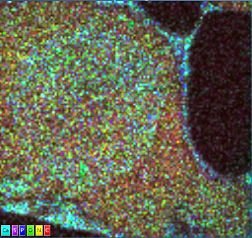
Striking ultrastructural contrast in unstained samples
Image: An unstained plant leaf cell fixed with aldehydes and embedded in LR white, section at 100nm thickness, showing the nucleus, vacuoles, tonoplast and cell membrane using elemental maps alone, no electron data is included in the image. Calcium in particular has distinctive distribution along the membrane and in the nucleus.
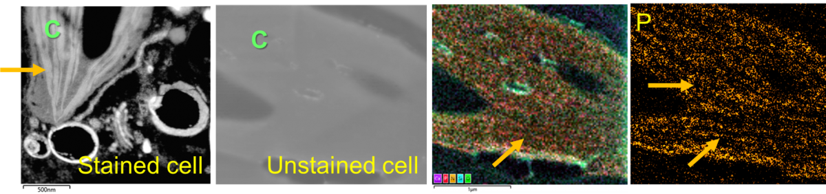
Arabidopsis thaliana leaf sample, stained (left) and unstained and embedded in LR white resin, sectioned at 100nm thickness Data was collected from 100nm thick resin embedded sections using 200kV (S)TEM and an Ultim Max TLE. EDS creates contrast in cells and tissues that have not been stained, facilitating the identification of cell components and avoiding the need for stain that may mask or distort normal structure and element maps. Thylakoid membranes (orange arrows) in a chloroplast (C) can be seen in the stained cell and in the phosphorus map of the unstained sample.
TEM data collected at the Centre for Ultrastructural Imaging, King’s College London
Speed & Sensitivity
REAL-TIME CHEMICAL MAPPING
10 nm Au film on SiN membrane heated from 0 - 800°C showing particle agglomeration. (Sequence sped up 20x)
FIB lamella showing Al2Cu precipitation and annealing when heated from 0 - 450°C. (Sequence sped up 20x)
EVEN AT ELEVATED TEMPERATURES
An increase in both solid angle and take off angle combined with windowless detection and Extreme electronics has led to uncompromised X-ray sensitivity. This means that the Ultim Max can now detect lower X-ray energies than ever before. The combination of Extreme electronics with the X4 pulse processor also allows for in situ EDS mapping and quantification at elevated temperatures > 800°C.
CALCULATE SAMPLE THICKNESS
Our easy to use quant routine allows for quantification by mass thickness. This allows you to use EDS alone to weigh nanoparticles with atomic accuracy. Using this method, it is now possible to calculate the thickness of a specimen and further understand the contrast in your images.
Brochures & Application Notes
Ultim Max TEM
Ultim Max is the next generation of Silicon Drift Detectors (SDD) utilising our Extreme electronics to generate maximised sensitivity with increased throughput. This powers AZtecTEM, the market-leading software that delivers unparalleled elemental characterisation performance in the TEM.
EDS is a mature technique that can be used for most specimens. EELS is more suitable for thin samples where the thickness is less than the inelastic mean free path of electrons in the material. Simultaneous acquisition of both signals is a powerful tool for materials analysis.
Semiconductor Mapping in the TEM - Solving peak overlaps in real-time
Elemental analysis of semiconductors is typically difficult due to strong overlaps of X-ray lines between commonly used elements and low concentrations of dopants. This brief shows how AZtecTEM solves these overlaps to achieve an accurate elemental analysis.
We are renowned for delivering outstanding support. Our global service hubs offer a full range of technical support to keep your detector, system and staff at maximum efficiency.
Keep your investment at peak performance. Multi-layered maintenance contracts suit your operational needs and budget.
Optimising you. Optimising your team. Omni-channel training enables everyone to deliver the right results every time.
Our global network of help desks guarantee a fast local expert response to any application or operational issue.
Our team of accredited support professionals proactively ensure your system is in optimal condition.
We’re with you every step of the way to future proof your investment and ensure onwards data and system compatibility.