17th March 2021 | Author: Dr Rosie Jones
How WDS can help ensure solder quality in electronics
The electronics sector greatly benefits from the inclusion of Wavelength Dispersive Spectrometry (WDS) and AZtecWave in their manufacturing processes. This is due to the requirement to accurately determine the concentrations of minor and trace elements present in electronic components, such as solders, packaging materials, interconnects, and coatings. Identifying the presence of impurities, element segregation, and precipitates is critically important to the performance of different electronic components.
WDS has higher peak to background ratios, compared to Energy Dispersive Spectrometry (EDS), meaning detection limits of <100 ppm can routinely be achieved for many elements. In addition, WDS has a higher spectral resolution compared to EDS. The spectral resolution of the Wave spectrometer, which is similar in design to WDS spectrometers used on electron microprobes, is typically 10x better than EDS. This enables full peak separation of all common overlaps, including all transition elements (e.g., Ti Kβ and V Kα). Therefore, adding a WDS spectrometer to an SEM brings greater analytical capability and versatility, and enables the accurate quantification of minor and trace elements. WDS is now integrated into the AZtec software platform, and recently I have been using the Wave spectrometer and AZtecWave to measure different compositions of Pb-free solders used in electronics. I present a couple of short examples here.
The first example I have been looking at is a tin-antimony
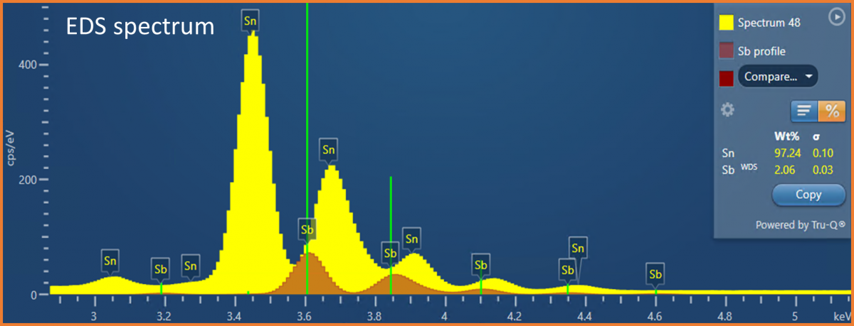
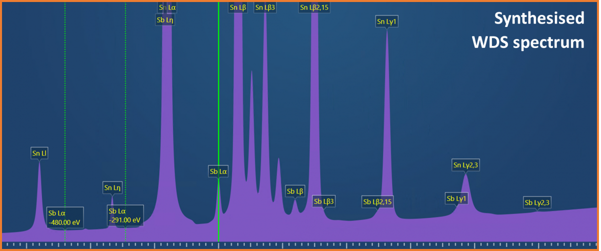
(Sn-Sb) solder, where Sn is the major element (~95%), and Sb is the more minor element (~5%). Antimony is often added to solders to increase the strength and to prevent the low temperature deterioration of tin (tin pest). Therefore, to test and evaluate the properties of a solder, accurate compositional determination is required. The analytical challenge presented is that energies of the characteristic X-rays for Sn and Sb are very similar (e.g., Sn Lβ = 3.662 keV and Sb Lα = 3.605 keV) causing significant peak overlaps in an EDS spectrum (see Fig. 1). These peak overlaps mean that it can be difficult to accurately quantify the concentration of Sb present in the solder, particularly if it is in low concentration (e.g., <5 wt.%) compared to the Sn, and a high level of certainty (i.e., low error) is required on the measurement. In some instances, the Sn and Sb appear to segregate, meaning that the Sb might only be present in trace amounts in some areas – making it even more tricky to measure. Fortunately, due to the higher energy resolution of WDS, it is possible to fully separate the Sn and Sb X-ray peaks (see Fig. 2).

Figure 1. An EDS spectrum acquired from the SnSb solder showing the X-ray peak overlaps in the EDS spectrum. The mini-quant shows a quantitative result obtained from a single point on the solder sample – showing an example of where the Sb concentration was less than ~5 wt%. In this example, WDS was used to measure the Sb concentration, and EDS was used to measure the concentration of the Sn at the same time – this is possible through the integration of EDS and WDS provided in the AZtecWave software.

Figure 2. A synthesised WDS spectrum showing the increase energy resolution of WDS compared to EDS (the energy range shown here is the equivalent to what is shown in Figure 1).
The second example I have been investigating is detecting and quantifying trace concentrations of Ni in Sn-Cu and Sn-Ag-Cu solders. The addition of a small amount of Ni (<0.5 wt.%) can change the properties of the solder and has some desirable effects, such as the reduction of void formation and interdiffusion of the Sn and Cu (e.g., Zhao et al., 2019). I used AZtecWave to analyse several Sn-Cu and Sn-Ag-Cu solders containing different concentrations of Ni. The concentrations of the major-minor elements present in the solder (i.e., Sn, Ag, Cu) were measured using EDS, and the minor-trace Ni contents were measured at the same time using WDS. Two example results are shown in the tables below. In these examples, Ni concentrations of 774 ±122 and 229 ±48 ppm were measured in the solders – demonstrating that WDS and AZtecWave can easily distinguish between solder samples with Ni concentrations <800 ppm with a precision of ±50 ppm in the best instance.
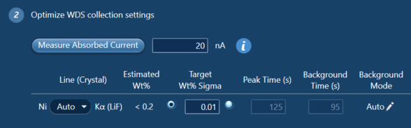
If you are interested in the analytical conditions used to measure the Ni concentrations - I used an accelerating voltage of 20 kV and a beam current of between 23 and 30 nA. Ni was measured using the LiF crystal and the WDS peak and background counting times were set by AZtecWave using the ‘3-way chooser’ (see Fig. 3) – this set the peak and background counting times based on the beam current, the expected Ni concentrations in the sample based on a previously acquired EDS spectrum, and the target wt% sigma (i.e., the level of uncertainty desired). This new feature of AZtecWave allows the user to make a much more informed decision about how long to count on the peak and background positions for. I have found that when measuring trace elements, counting for longer on the background is what often improves the error associated with the result.

Figure 3. A snapshot of the AZtecWave interface showing the automatic setting of peak and background counting times based on the measured absorbed current, the estimated wt% of the element in the sample, and the target wt% sigma. Alternatively, if you know how long you want to count for, AZtecWave will calculate the wt% sigma you can expect on the result with the measured absorbed current.
In this blog post, I have demonstrated how WDS and AZtecWave can be used to identify and quantify minor-trace elements present in solders used in electronics. If you would like further information on AZtecWave, please get in touch today.
Find out more