A look to the future - investigating the potential of the EBSD technique with combined focused ion beam
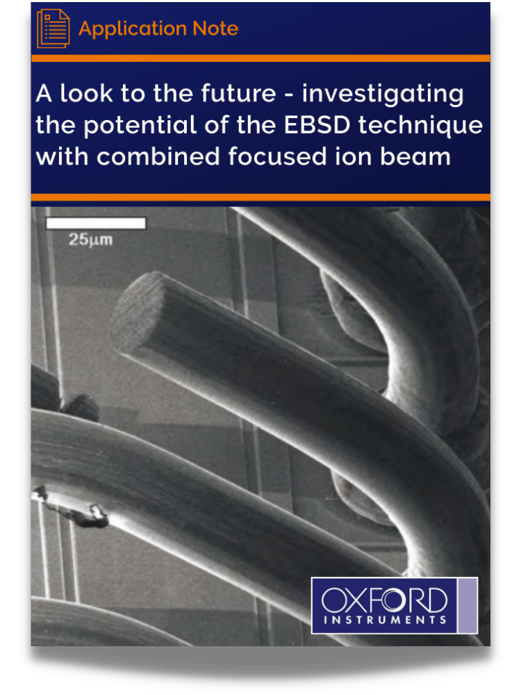
The recent emergence of integrated focused ion beam (FIB) instruments and scanning electron microscopes (SEMs) has caused considerable excitement in the materials and nanotechnology world. FIB-SEMs (commercially known as Dual-Beam or Cross-Beam instruments) allow the sectioning and shaping of samples on the nanometre scale, with integrated high-resolution imaging. The potential of this technology, with the continuing drive towards miniaturisation and nanotechnology, is considerable, with applications in many fields. An added benefit for use with EBSD analyses is that the cut surfaces are ideal for obtaining diffraction patterns, with no further preparation necessary. Integrating EBSD technology into FIB-SEM instruments is not simple for 2 reasons. Firstly, the cross-over point of the electron and ion beams is at a very short working distance (5-8mm), and secondly, the ion gun and associated gas injectors can obstruct the EBSD detector during insertion. However, Oxford Instruments EBSD HKLNordlys detector combines a tapered nose design with specialised tilting interface plates to allow EBSD analyses at the electron-ion beam cross-over point (such as in the image above). This opens up a whole spectrum of new EBSD applications. In this application note, we look at 3 examples of combined EBSD and FIB-SEM, illustrating the unique opportunities afforded by the sectioning capabilities of such instruments.
By downloading this application note you will see:
- Three brief examples of the application of the EBSD technique with combined FIB-SEM instruments
- The potential for slicing and preparing surfaces on very small or difficult samples
*Please note this application note refers to Nordlys. This has since been upgraded to Symmetry S3.
Get my copy!


