Improving the spatial resolution of EBSD using transmission Kikuchi diffraction in the SEM
It is becoming increasingly important to be able to characterise materials on the nanoscale. Despite significant technological developments in recent years, the EBSD technique is still limited by the pattern source volume to resolutions in the order of 25-100 nm; this is insufficient to measure accurately truly nanostructured materials (with mean grain sizes below 100 nm). A new approach to SEM-based diffraction has emerged, namely using an electron transparent sample coupled with conventional EBSD hardware and software. This technique referred to as transmission EBSD (t-EBSD: Keller and Geiss, 2012) or SEM transmission Kikuchi diffraction (TKD: Trimby, 2012) has been proven to enable spatial resolutions better than 10 nm and is ideal for routine EBSD characterisation of both nanostructured and highly deformed samples.
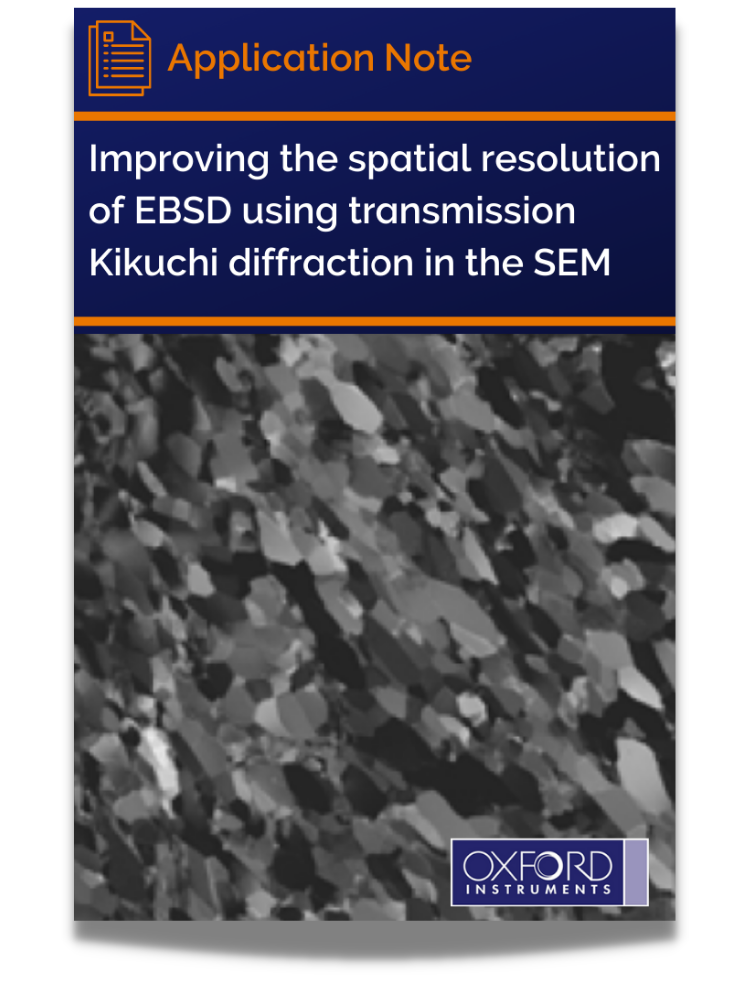
This application note describes the set up required for working with an EBSD system in transmission mode, using a NordlysNano EBSD detector and AZtecHKL. It illustrates the application of TKD to a nanostructured nickel sample and a highly deformed stainless steel, both of which were impossible to characterise using conventional EBSD.
*Please note, this application note refers to NordlysNano. This has since been updated to Symmetry S3.
Get my copy!