10th March 2021 | Author: Iain Anderson
Why a phosphor screen is so important in EBSD
Since the 1980s, the unsung hero of EBSD systems has been the phosphor. That innocuous film, sitting on a piece of glass and behind a thin coating of aluminium, is responsible for turning the incident pattern of electrons into a pattern of visible light which can then be imaged by a camera. Over the past few decades, camera technology for imaging this visible light has evolved, and thanks to the phosphor EBSD as a technique has been able to take advantage of all the new technology. Culminating today in our CMOS detectors which are built using a bespoke sensor optimised for EBSD.
Not all electrons are created equal
It’s straightforward to consider that the phosphor turns an electron signal into photons, but if we look closer there’s more happening here than you might imagine!
A good phosphor may be somewhere between 10-20% efficient at converting electron energy into photon energy. For a green phosphor, this means that a single 20keV electron will produce well over 1000 photons, and a 5keV electron well over 250 photons (the phosphor response remains linear down to low energies). The phosphor is actually a pretty efficient transducer.
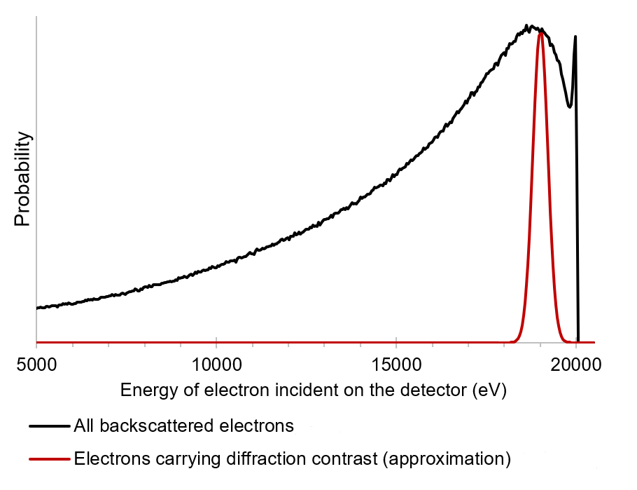
Things then become interesting when you consider that the useful information in each EBSP is carried only by diffracted electrons and that these diffracted electrons have a very different energy distribution to that of the bulk of the backscattered electrons which also strike the screen but produce only a noisy ‘background’ (Figure 1). I like to think of these two groups as ‘good’ and ‘bad’ electrons!
Figure 1: Electron energy distributions. Monte Carlo simulations1 for Si sample, 70 tilt, 20keV beam energy
Knowing that the ‘bad’ electrons are predominantly of a lower energy than the ‘good’ electrons, and that the phosphor is simply converting electron energy to photon energy. It follows that the screen will actually glow less brightly when it is struck by a ‘bad’ electron that it will when hit by a ‘good’ electron – the phosphor is basically a filter, creating more signal from the electrons we want to image than it does from electrons which are only background noise!
Electrons are not all created equal and we should not count them as such, so it’s reassuring that the phosphor is working on our behalf to weed out some of the ‘bad’ from the ‘good’. In a well-designed system, the energy discrimination offered by the phosphor contributes significantly to enhancing the sensitivity of an EBSD detector.
Capturing every photon
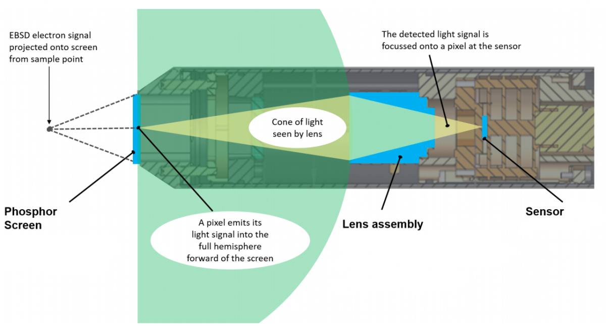
Of course, all those photons are only useful if they reach the camera sensor, and that’s where our unique fibre-optics come in. With the phosphor coating directly attached to a fibre-optic plate we ensure that a high proportion of the photons generated are transferred to our CMOS sensor. When comparing this with traditional camera optics (Figure 2) this is an incredible advantage.

Figure 2: 2-D Cross-section of a conventional EBSD camera highlighting the main optical elements. Imagining this in 3-D, we can understand that the cone of light seen by the lens (yellow) is a just a tiny fraction of the light emitted into the 2π sr hemisphere forward of the phosphor screen (green)
Even with the best conventional lens assemblies, more than 99% of the emitted light is lost, never being transferred to the sensor.
Using fibre optics in place of a conventional lens, we have been able to increase the light-gathering efficiency of the camera inside our Symmetry EBSD detector by a factor of 10. The sensitivity advantage of collecting all that light using fibre-optics is what enables work on beam sensitive samples like organic perovskites. The very same advantage also means we can run at maximum speed without needing high beam current.
Softening the Blow
Back in 2017 I was working with our manufacturing and development teams to test our first ever Symmetry detectors and prove their performance capabilities, before they were shipped on to customers. With the basic subsystems tested, the final thing to do was get the detector onto a microscope and use it to collect real EBSD data.
After the first few detectors passed with flying colours the process became routine and a couple of absent-minded mouse clicks later, having already disabled the proximity detection, I had driven the sample stage directly into the front of the phosphor screen.
As I sheepishly carried the damaged product back for repair, I was reassured by our applications experts that destroying a phosphor screen is a rite of passage for all EBSD users. We’re all only human and mistakes happen when working with tilted samples in microscope chambers with poor visibility.
Figure 3 – Early Symmetry detector with pristine phosphor screen, photo taken moments before my induction into the ‘damaged screen club’
Now a fully signed-up member of the ‘damaged screen club’ my spirits were lifted by the speed with which the damaged screen could be removed and replaced, an operation that was finished in minutes. Notably, the same reassurance also carries through to experiments which may result in contamination or damage to the screen - whether that is from sample degassing during heating experiments, or redeposition of milled material from a FIB.
That of course highlights the second special power of a simple phosphor screen. That such a vital, powerful, and fragile component is truly a consumable assures me that my mistakes as a user will never be too expensive to fix.
I have little doubt that product launches will continue to be dominated by high profile glamourous specifications about camera megapixels and maximum frame rates while the phosphor will continue quietly doing its remarkable work at the heart of EBSD systems everywhere, but today I celebrate the humble phosphor screen!
Want more technical detail about the sensitivity of EBSD detector systems… why not download our technical note High Sensitivity EBSD Detectors?