Taking the manufacture of any product from prototype to mass production is a complex process that can introduce variability and defects. All manufacturers introduce quality control measures to ensure that each product that leaves their factory meets a specification. QC is a confirmatory process which results in a pass or fail for the individual product. Depending on the product and the manufacturer, when a product fails the QC process, it is investigated further by the FA department to establish the failure mechanism. This process is also carried out on products that have been returned by end users. It is vitally important that any analysis carried out is done so in a timely fashion.
In the beginning
Historically optical microscopy was seen as the ‘go to’ technique for Quality Control and Failure Analysis issues in production processes. It was seen as a quick and easy technique that can be used without extensive training or technique knowledge. As the nature of the analysis became more demanding, then so did the requirement for greater expertise and advanced instrumentation. For example, immersing glass fragments in different media under the optical microscope will render them opaque. This technique is used to measure the refractive index and, in turn, help identify the source of the glass contamination, for example, and polarised light can be used to identify different types of asbestos. But both these applications require more advanced technical knowledge.
More automated methods were also used to look at key parameters from large sample sets, e.g. performing particle size analysis on particles found in airborne filters or engine wear particles in oil. Optical images would be digitised and analysed with particle analysis software to measure the mean particle size distribution.
EDS meets new demands
As production processes became more complicated, the demand for greater information from QC and FA meant that optical microscopy could no longer deliver the necessary information. The introduction of the Scanning Electron Microscope with Energy Dispersive Spectroscopy (EDS/EDX) could easily fulfil these new demands.
Although various types of contamination could be identified with the optical microscopy methods of the day, they weren’t conclusive or comprehensive. Being able to obtain the elemental composition via EDS meant that contaminants could be identified conclusively. The use of SEM-EDS also meant that users could now analyse smaller features that were impossible to see using optical methods. The availability of motorised stages and particle analysis packages within the EDS software meant that large sample areas could be analysed automatically, even running overnight.
With the requirements for increased capability and complexity, came the need for any solution to be as simple and straightforward as possible. This was due in part to a general lack of SEM-EDS expertise in the users performing QC and FA analysis in production facilities and in part because of a demand to increase productivity. So, from an EDS point of view, the software needed to be easy to use, and the results needed to be acquired quickly, without compromising accuracy and reliability.
The current day
Moving to the current day, the jobs that are carried out by SEM-EDS in QC and FA may include determining the provenance of contaminants or investigating the failure mechanism of a delaminated coating. The workflow could involve the acquisition of an image and a simple spectrum as we can see below.
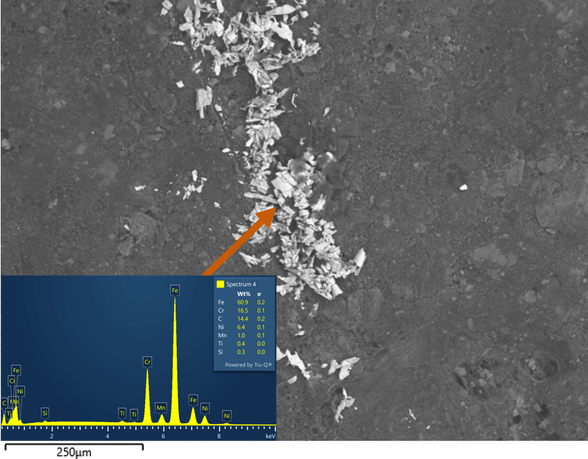
Analysis of a pharmaceutical tablet that was found to have a discolouration on the outer coating. SEM-EDS analysis quickly identified the discolouration as fragments of a stainless steel that could potentially be traced back to machinery on the production line.
More complicated analysis may include automation over a large sample, which could constitute the acquisition of up to 10,000 individual areas. Each individual area could involve the acquisition of a full SmartMap with an EDS spectrum recorded for each pixel. Alternatively, individual particles can be detected in each area and both EDS and morphological data can be acquired. The example below is from one such example from a battery sample.
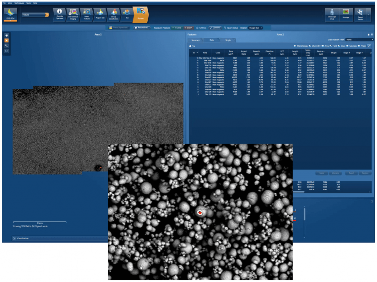
Automated particle analysis of a battery powder sample – hunting for contaminants in an NCM powder.
This blog can of course only provide a glimpse into the use of SEM-EDS in QA and FA processes. We will go into much more detail in our upcoming webinar ‘The use of EDS for QA and FA within production processes’ where we will show worked examples from several different industries. Please join us on Thursday 9th June 2022 – you can get to the registration page here.