During my geology studies, I often needed to access an electron microprobe (EPMA) to collect quantitative elemental data for the minerals present in the volcanic/igneous rock samples I had collected on fieldwork.
The university’s EPMA facility I had access to was extremely busy, and I often had to wait several months before being able to acquire my data. This had a knock-on effect, as I needed the EPMA results to decide which samples were best suited for further isotopic analysis.
What would have helped me in this situation would have been the option to conduct preliminary trace element analysis using an SEM equipped with a wavelength dispersive spectrometer (WDS or WDX). In comparison to the EPMA, my department’s SEM was significantly easier to access, as well as being cheaper to use, making it more affordable for my limited PhD funds.
The EPMA is a dedicated instrument for elemental microanalysis using wavelength dispersive spectrometry (WDS). EPMA’s are typically used for quantitative, in-situ measurements of the elemental composition (major, minor and trace element concentrations) of solid samples. One way of offering EPMA-like capabilities on an SEM platform is with the Oxford Instruments Wave
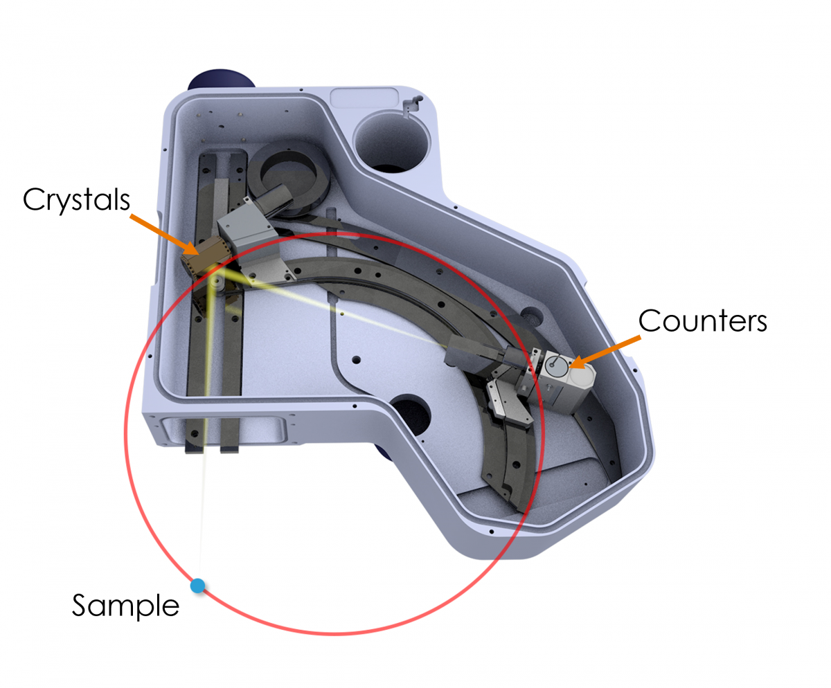
spectrometer. The Wave spectrometer has a very similar design to WD spectrometers on EPMA instruments – it has fully focussing Rowland circle geometry with curved crystals (see figure below). This spectrometer design provides the best spectral resolution available on the SEM, and in some cases surpasses that achieved by EPMA.

AZtecWave delivers key benefits
The high spectral resolution of the Wave spectrometer delivers two key benefits to the SEM:
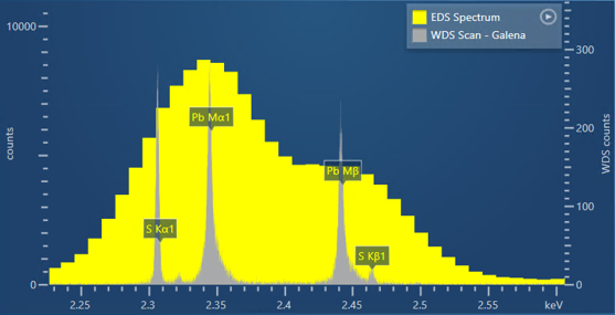
- Wave can resolve overlapping X-ray peaks in the EDS spectrum, and therefore improve accurate element identification and quantification.
- Wave delivers higher peak to background ratios and therefore lower detection limits (<100 ppm for many elements). Consequently, Wave makes it possible to accurately quantify trace elements (defined as <1000 ppm) with an SEM.

An electron microprobe typically has five WD spectrometers mounted vertically on the column. As WDS is a serial technique, each spectrometer can only measure one element at a time. Having multiple spectrometers means multiple elements can be analysed simultaneously (i.e. multi-collection).
Combining WDS with EDS saves time
An SEM column can only accommodate one WDS, making elemental analysis of multi-element samples a time-consuming endeavour. To address this limitation, we have designed AZtecWave. Using AZtecWave, WDS can be conducted in combination with energy dispersive spectrometry (EDS). EDS is a faster technique, as it can measure all elements present in a sample simultaneously, and the EDS detector achieves higher count rate due to its higher solid angle. In practice, this means that major-minor elements, and those unaffected by peak overlaps, can be quickly and accurately quantified using EDS with AZtec TruQ spectrum processing. That leaves WDS to be utilised only where it is needed - for accurately quantifying trace elements and resolving X-ray peak overlaps.
Substantial support
Although the AZtecWave WDS/EDS system on a SEM is not equal to a fully-fledged electron microprobe, it does go a substantial way towards it and can provide an excellent support option for a busy EPMA. An AZtecWave WDS/EDS system can support an EPMA facility in the following ways:
- You don’t need to be an expert to use AZtecWave
Electron microprobes are inherently complicated to setup, use and maintain, and therefore most EPMA labs have a full-time dedicated operator. SEMs tend to be easier to operate, and acquiring compositional data with EDS is typically much more straightforward. Far more people have experience operating and collecting data on an SEM with EDS than on an electron microprobe. Therefore, conducting WDS analysis on an SEM with AZtecWave is less of a ‘jump’ compared to moving to EPMA. This is enhanced by all the features we have incorporated into AZtecWave to make it easy for users of all experience levels to obtain accurate results. One of the key ease-of-use features is our software technology that takes real-time information from the SEM-EDS system to automatically optimise the WDS (+EDS) setup and analysis. Also included are step-by-step instructions, embedded help videos, and inbuilt spectrometer performance checks.
In addition, not only is WDS with AZtecWave easier to use, but it is also easier to train users on, making it an excellent training tool for users who are unfamiliar with WDS analysis. Going back to my experiences as a PhD student learning the fundamentals of WDS, I think I would have found learning WDS analysis on an SEM much easier and less intimidating than EPMA.
- Some analysis jobs can be adequately solved using SEM-based WDS
For geologists, one of the first levels of analysis that is commonly required is the determination of the major-trace element composition of the minerals present in a suite of rock samples. This gives lots of useful information, including helping to establish the exact minerals present and which samples to focus on for further analyses. In minerals, there are often only a few elements of interest which might be present in trace concentrations. An SEM-EDS system with AZtecWave could be used to conduct the majority of these analyses, particularly when there is a limited number of trace/overlapped elements involved. In turn, this frees up time on the EPMA, so it can be more efficiently used for the jobs that truly require it.
- Easy combination with high resolution imaging and other SEM-based techniques Another advantage of AZtecWave is that, because it is on an SEM, WDS analysis can be easily combined and correlated with high resolution electron imaging (e.g. SE, BSE), often down to the nm level; other imaging techniques such as cathodoluminescence (CL);, and other SEM-based techniques, such as electron backscatter diffraction (EBSD). This level of flexibility and correlation with other techniques is not possible with an EPMA, which has been designed for the most optimal WDS analysis.

- AZtecWave can be used for initial investigations and sample screening before EPMA analysis As discussed in the previous point, an SEM with AZtecWave provides a highly flexible instrument for sample imaging and analysis. Firstly, because the analysis is being conducted on an SEM, much larger samples can be investigated – the only limitations are that of the SEM stage and chamber. In addition, the sample can be titled using the SEM stage, perhaps to get a flat surface parallel to the bottom of the pole piece, or to perform correlated EBSD analysis, which typically requires the sample to be tilted to 70 degrees. Secondly, because the Wave spectrometer is mounted on the SEM column at an inclined angle, the plane of the Rowland circle is broadened, thus making the WDS analysis less sensitive to sample height compared to EPMA with vertically mounted spectrometers. As a result, the sample can be adequately focused using the SEM secondary electron image, and there is no need for careful focusing using an optical image like on an EPMA. This also means the SEM-system can tolerate a limited amount of topography on the sample surface and still produce good results. These features combine to make an SEM with AZtecWave highly suitable for initial sample investigations, for example to identify which samples are worth preparing further and worth conducting EPMA analysis on. In addition, the WDS analysis conducted using the Wave spectrometer is directly comparable to WDS data obtained on an EPMA, providing a good indication of what can be expected.
- Financially favourable
Finally, when it comes to cost, an SEM-EDS system with AZtecWave provides a cost-effective solution for increasing analytical capability. It provides the means to accurately identify and quantify trace elements and those affected by peak overlaps in the EDS spectrum, without the need for (another) EPMA. As well as the initial cost, the expense associated with running and maintaining an SEM is also likely to be significantly lower than those associated with EPMA.
After reading this blog, I hope you agree that having an SEM with AZtecWave can provide an excellent support option for your EPMA facility.


