Applying nanomanipulation to the EBSD analysis of a gold wire
As the trend towards miniaturisation and nanotechnology increases in microelectronic devices, a key growing requirement is the microstructural understanding of materials at the nanoscales to produce reliable products. Detailed failure analysis on this scale typically requires a focused ion beam (FIB-SEM) combined with nanomanipulator tools to extract and lift-out specific regions of interest or failure. Analytical and structural characterisation of the lift outs is then usually undertaken in a TEM. This analysis is complex and there are limitations in the size of area which can be examined. Alternatively, the technique of electron backscatter diffraction (EBSD) can be applied for these applications, either in the FIB-SEM or the FEGSEM fitted with EBSD systems.
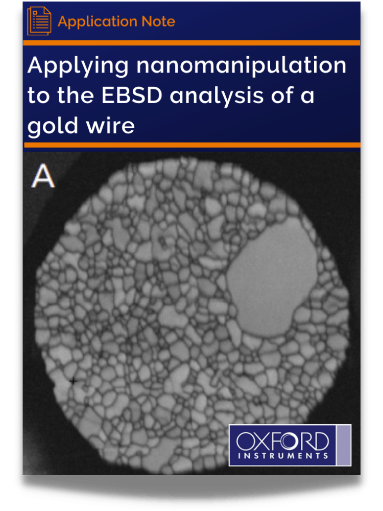
This application note describes a method of combining Oxford Instrument’s OmniProbe tools and AZtec EBSD system for the manipulation and analysis of a 5μm diameter gold microelectronic wire sample.
By downloading this application note you will see:
- The experimental procedure, using OmniProbe tools for sample preparation, cutting and transfer procedure
- EBSD analyses including EBSD acquisition parameter details
*Please note, this application note mentions OmniProbe 100 & NordlysNano which have since been upgraded to OmniProbe 400 & Symmetry S3 respectively.
Get my copy!