SEM can be used to analyse a wide range of samples at magnifications between 1 and 2,000,000 times. During day-to-day routine analysis, EDS is typically a point and click process, returning elemental information quickly and easily. However, there are scenarios that require changing the microscope settings, sample preparation routines and type of analysis to acquire more complex data.
An example of this is nanometer scale, high resolution EDS mapping.
High resolution EDS mapping can effectively be acquired using 3 different SEM acquisition routines are:
- Conventional High kV SEM
- Low kV SEM
- STEM-SEM
Each routine has different advantages and disadvantages which influence what approach is best for the sample being analysed.
Conventional High kV SEM
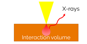
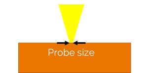
The conventional approach to SEM EDS analysis utilises high accelerating voltages, typically 20kV, with large working distances. The result is a spatial resolution (the maximum detectable feature size) that is limited by the size of the electron probe as it forms on the sample.
This is by far the easiest approach for novice SEM users to acquire high
resolution EDS maps, as most SEMs are aligned and operated at 20 kV with
standard EDS detectors optimised for this geometry. The main downfall of this
method is that the electron probe is quite large, returning the worst spatial resolution, with the maximum feature size that can be mapped as approximately 1000 nm (1 µm).
- 20 kV accelerating voltage
- 10-15 mm working distance
- Spatial resolution limited by probe size of the SEM
- Maximum EDS map spatial resolution ≈1000 nm
Low kV SEM
- 1.5-10 kV accelerating voltage
- 4-8 mm working distance
- Spatial resolution limited by the interaction volume
- Maximum EDS map spatial resolution ≈5 nm

By lowering both the accelerating voltage and working distance, the spatial resolution of the SEM is greatly improved, as the microscope forms a finer probe with the electron beam. Low kV resolution improvements can be seen even at relatively high voltages like 10 kV, but to achieve the best resolution, an accelerating voltage of 5 kV or below should be used.
This returns an EDS mapping spatial resolution that is orders of magnitude greater than high kV, with features between 100 and 5 nm now resolvable. The accelerating voltage choice now governs the spatial resolution, as it defines the interaction volume and where X-rays are being generated.
STEM-SEM
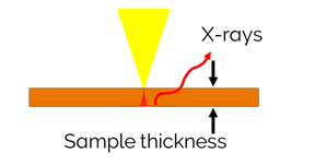
An alternative approach to high spatial resolution EDS maps is through STEM-SEM, in which electron transparent samples, with thicknesses ≤ 100 nm, are utilized to achieve sub 10nm maps. By operating at large accelerating voltages, typically 30 kV, electrons are transmitted through a sample and imaged using a STEM detector, in turn this generates X-rays for EDS analysis. We see a significant resolution improvement when analysing these samples due to the EDS spatial resolution not being degraded by the interaction volume as there is no bulk material. This technique returns high resolution EDS analysis very easily, however, the requirement for an electron transparent sample means that sample preparation can be more complex and time consuming.
- 20-30 kV accelerating voltage
- 6-10 mm working distance
- Spatial resolution limited by sample thickness
- Maximum EDS map spatial resolution ≈5 nm

When comparing high-resolution EDS maps of a Ni super alloy sample (below) acquired using low kV EDS and STEM-SEM, you can see for both techniques features < 20 nm are easily observed. However, for this material a significant resolution improvement is observed in STEM-SEM mode.
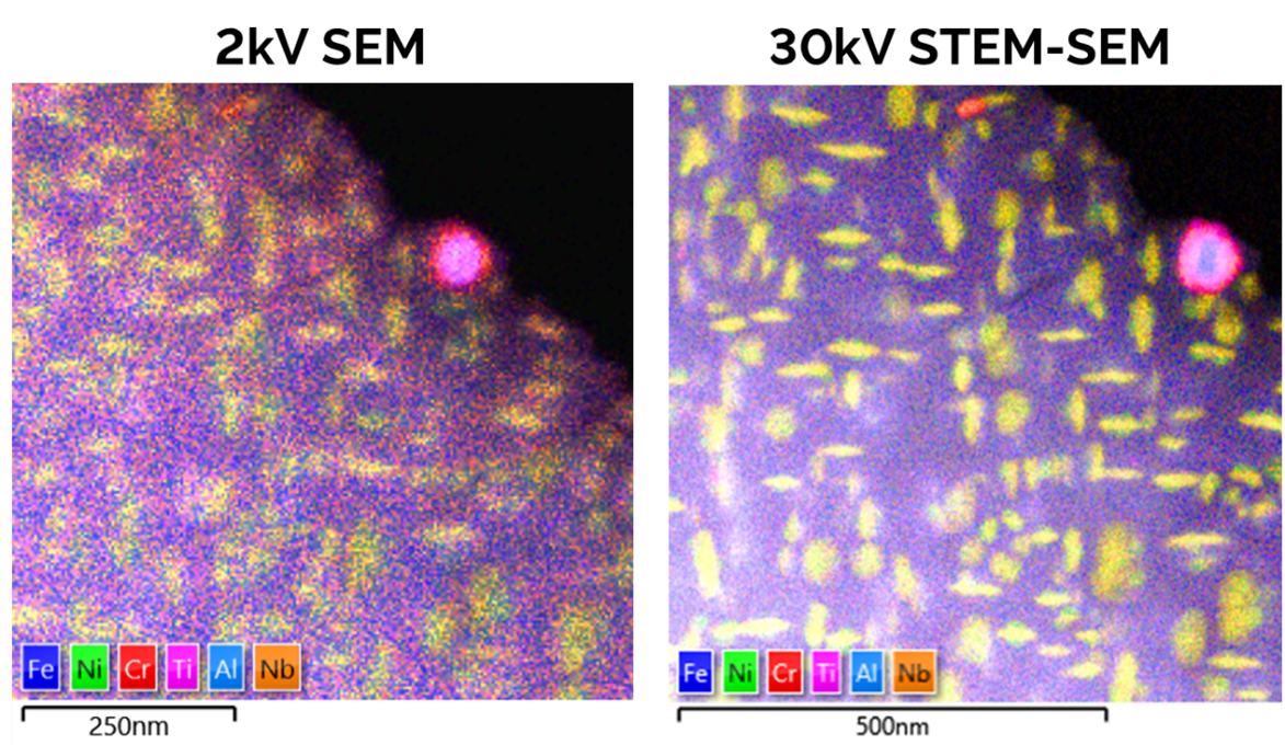
High-resolution EDS mapping can be achieved using a range of approaches within the SEM. When deciding what technique to utilise, the sample and microscope conditions are the limiting factors. By changing analysis mode away from conventional 20kV SEM, we can achieve spatial resolution improvements that are orders of magnitude greater than standard 20kV SEM analysis.