Incredibly, it has been almost 3 years since we launched the world’s first CMOS-based commercial EBSD detector, Symmetry. I wrote at the time that “in my opinion, the age of the CCD detector in EBSD is over” and I remember getting some criticism from researchers in the EBSD community – clearly, they thought it was just marketing hyperbole. However, fast forward 3 years and we can see that Symmetry really is leading the way in the EBSD market.
There are always small tips and tricks that we can learn about an EBSD system, and here I have picked out a couple of pointers that can help you to get even more out of your detector.
1. When to use the detector elevation control
The simple answer to this is “every time”! This is a fantastic feature that ensures you are working with the best geometry every time you collect EBSD data from your samples. The way it works is simple – in the detector control settings within AZtec there is a tab labelled “Elevation” – here you define the movement (in mm) up or down from the standard elevation position:
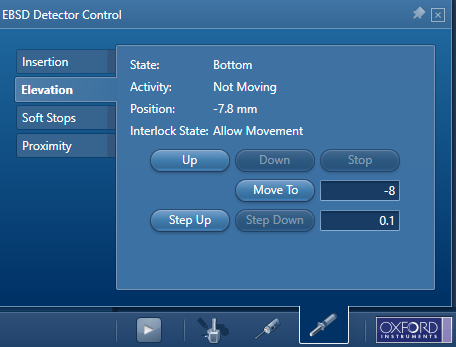
The limits would have been set by the engineer upon installation, with the upwards motion usually limited by the EDS detector position, with greater freedom of movement downwards. Once you set the desired position and press “Move To” (or simply select “Up” or “Down”), the motorised elevation control will tilt the detector to the desired position and AZtec will automatically adjust the calibration so that indexing will be unaffected. So that’s all very easy, but when might you benefit from altering the detector elevation? Here are the most common cases:
Analysing large samples
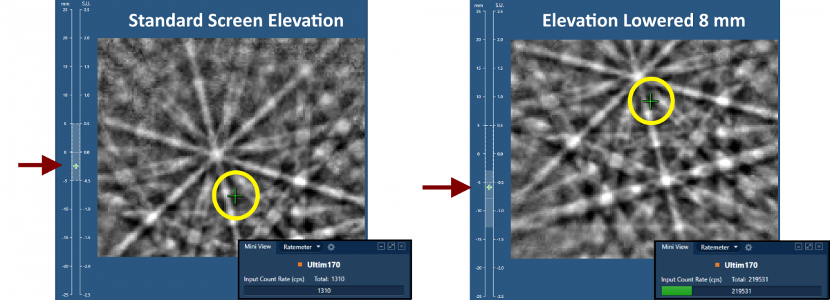
We all know the frustration when trying to work on a large sample at the installation-set “optimum” EBSD working distance and being unable to move to all parts of the surface for fear of colliding with the SEM pole piece. Now we can simply move the sample to a longer, safer working distance and lower the detector elevation until it is at the ideal geometry for EBSD. On the Optimise Detector step in AZtec you can use the elevation graphic next to the EBSP display to see the relationship between the sample and the phosphor screen – remember that the optimum pattern centre position is about ¾ up the screen. Lowering the EBSD detector position will also allow you to collect plenty of X-rays with your EDS detector, although you may benefit from retracting the EDS detector at least part of the way. The images below show the benefits of optimising the sample-detector geometry, in this case for a large martensitic steel sample. The left-hand image shows the EBSP at the standard screen position: note the very low pattern centre (yellow circle), the screen elevation graphic to the left (red arrow), the weak signal at the top of the EBSP and the complete lack of any X-ray counts. Lowering the screen by only 8 mm (right-hand image) optimises the pattern centre position giving a much better EBSP, as well as > 200k X-ray counts per second!
Transmission Kikuchi Diffraction (TKD)
Geometry is all-important for successful TKD analyses: usually you will want to work with the sample at a short WD (often ~ 5 mm) and close to horizontal. To get the best diffraction pattern the detector will need to be fully inserted and with the sample approximately level with (if horizontal) or a few mm below (if back-tilted 10-20°) the top of the phosphor screen. You can easily adjust Symmetry’s elevation to get the optimum position – if you start to see some shadowing (as shown), then either back-tilt the sample away from the detector or lower the detector elevation by a few mm. Simple!
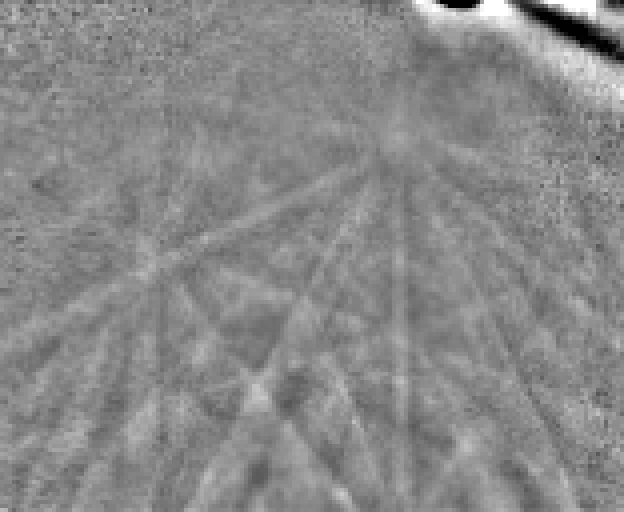
TKD pattern with shadowing – a slight change in sample tilt or detector elevation will eliminate this problem
Changing beam energy or material atomic number
These 2 parameters are closely linked, as they affect the variation in diffraction pattern intensity in a vertical direction. When using a higher acceleration voltage or analysing low-Z materials, the most intense diffracted signal will be projected relatively low down – in such cases it can benefit the analyses to lower the phosphor screen elevation by a few mm. For low acceleration voltages or when analysing high-Z materials, the electrons will be scattered through a higher angle and the diffraction pattern will be projected higher up – so move the phosphor screen up!
EBSPs from a grain of the mineral zircon (ZrSiO4) collected at the same geometry (WD and detector position). Left – 10 kV accelerating voltage. Right – 30 kV accelerating voltage. Note the weak signal low down in the low energy EBSP – here the data quality would be significantly improved by moving the detector upwards by 5 mm.
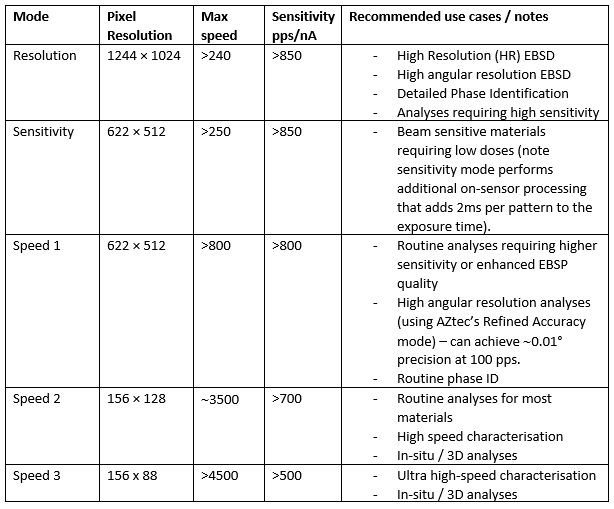
2. Choosing the best detector mode
Symmetry S2 has 5 separate modes of use: Resolution, Sensitivity, Speed 1, Speed 2, and Speed 3. Each mode has its main target applications, as detailed in the table below. My personal go-to mode is Speed 2: the EBSP resolution is sufficient to ensure great data from almost any sample, plus the increase in speed helps with all types of analysis. Also, if you want to save the diffraction patterns, it’s not so punishing on disk space! However, there are times when I will switch to the other modes, particularly if I require additional sensitivity or will benefit from the added pixel-resolution of the patterns (such as when using AZtec’s refined accuracy mode), or if speed is the key concern in which case I will switch to the new Speed 3 mode, capable of speeds > 4500pps.
Note that we have started to specify sensitivity values, here using the units of patterns per second per nA (pps/nA). All EBSD manufacturers tend to claim that their EBSD detectors are “high sensitivity”, but with no values to back up their claims. We believe that the fibre optics inside all of our CMOS detectors provide the best sensitivity of any detector currently on the market, and we want to specify what this means. So, these values are taken from a typical installation from a well-prepared Ni or steel sample and provide an indication of what sensitivity should be possible:
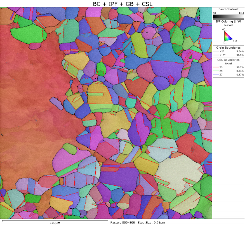
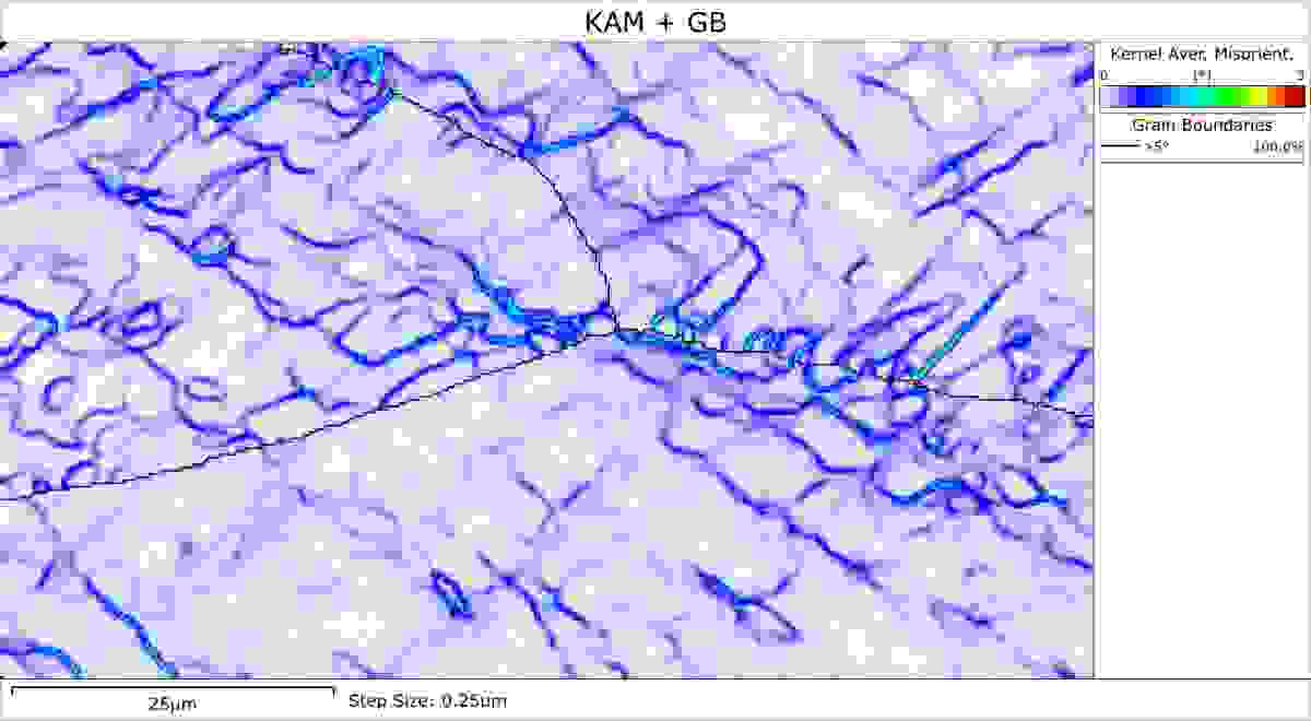
So what does this mean in terms of analysing your samples? Well, simply put, the S2 will deliver the flexibility to get the best data from any type of sample. Take a look at the 2 examples below – the first is a Ni sample, analysed using Speed 2 mode at over 3000 patterns per second using only 4 nA beam current. The second is a kernel average misorientation map showing dislocation cells in a deformed and briefly annealed Al-Mg alloy, collected using Speed 1 mode at ~100 patterns per second with refined accuracy indexing (the orientation change across many of the cell walls is < 0.05°).

Taking the time to select the best mode will deliver the results that you need – you have unrivalled flexibility with your Symmetry S2, so why not use it?
Sign up for our mailing list to be notified when the next Symmetry S2 Tips and Tricks blog is released, focussing on setting the exposure time, collecting forescatter images and the benefits of retracting your detector. In the meantime, good luck with your analyses and don’t forget to let us know if you have any great, exciting results.