There are many reasons why an electrical connection on a Nanomanipulator may be desirable. Here we cover not only various high precision electrical testing methods such as EBIC and EBAC but also show how an electrical connected probe can be used to enhance the imaging capabilities of a FIB-SEM.
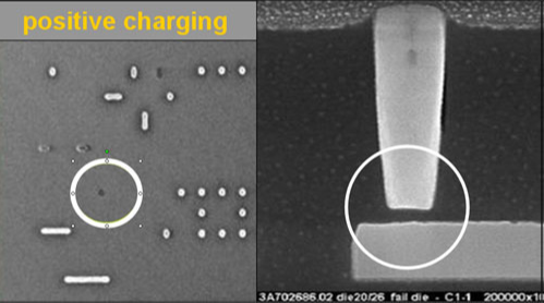
The sample in an electron microscope is always part of an electrical circuit with the current supplied by the electron beam being dissipated through a grounded sample stage. If the pathway is disrupted for example by an insulating sample in vacuum, the electrons from the beam charge up the sample. The charge builds up in the sample then interacts with the electron beam and prevents us from obtaining high quality images. This is usually overcome by applying a conductive coating to a sample or by working under low vacuum conditions where the ionised gas atoms present around the sample dissipate the charge. However, neither coating nor low vacuum mode is ideal for working in a FIB-SEM as the coating is often removed at least locally by ion milling sample and a high vacuum is required for good quality deposition and milling with the ion beam. Under such circumstances, an electrically connected and grounded probe can be placed close to the area that is being imaged and the charge induced by the electron beam can be dissipated through the probe, neutralising any charge build up.
This improves analytical results, where charging affects the electron beam landing energy, resulting in better quantitative EDS. The method can also be used to improve GIS deposition and imaging quality. A good example of this can be on an uncoated rock sample, but also works for many other samples such as glasses, electrical devices, and biological samples.
Uncoated geological sample imaged while charging and locally grounded with an OmniProbe.
All current OmniProbes include not only an electrical connection to the probe tip but also a ±10V power supply integrated into the controller. This enables two important capabilities: contact detection and voltage contrast imaging.
Probe-Sample Contact Detection: As mentioned above, the sample is usually electrically connected to the stage, to avoid charging. If the probe tip is biased and the voltage measured, a sudden drop in the voltage can be interpreted as the probe having contacted a conductive sample. This signal can be set to disable probe motion. In order not to activate the microscope stage touch alarm (which often use a similar method of contact detection), it is important to set the voltage on the probe tip to match the stage bias.

Image from the OmniProbe software showing electrical contact warning and the option to override the warning.
Imaging electrical properties in your sample
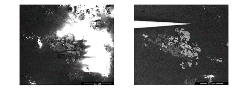
To reveal defects in electrical devices or even within electronic materials, electrically enhanced imaging may be desirable. One way to do this with an OmniProbe is to apply a voltage to the sample through the probe tip and perform voltage contrast imaging. Image contrast depends on the electrical connectivity of the different sample regions relative to the probe and can therefore be used to reveal broken or faulty connection in electronic circuits on the nanoscale. The example below (taken from J Mater Sci: Mater Electron (2011) 22:1523–1535), shows the identification of a fault, subsequent FIB cross-sectioning showed it to be an open circuit.

Voltage contrast imaging shows location of open circuit, FIB cross-section confirms this.
More advanced characterisation of electrical devices uses parametric analysers or source measurement units (SMU’s). I will not attempt to discuss these in detail here as each process could take several blogs to scratch the surface. The key point of analysers is that they can apply a set voltage and current while also measuring the response (as opposed to traditional measurements of applying a voltage and measuring current, or vice versa) to characterise a device. For current generation semiconductor devices, the measured signals are often in the picoamps. To ensure a good signal the electrical connection must be upgraded to a low noise electrical test option. This is separated from the probe control electronics and uses a dedicated connection on the OmniProbe body to minimise signal noise. Testing can often involve multiple probes.
For electron beam test methods there are two main types, electron beam induced current (EBIC) and electron beam absorbed current (EBAC). Although others do exist, they are not as widely used. Both these methods measure the current (usually with a high bandwidth picoammeter and a scan generator) generated by the electron beam in the sample and output the result as a current map. The key difference between EBIC and EBAC is the physical interaction which occurs in the sample. EBIC signals are usually several orders of magnitude larger than EBAC.
EBIC occurs when the electron beam interacts with a P-N junction (a semiconductor) and induces a current. This analysis is often used in semiconductor manufacturing and research of structures such as solar cells. The method works for both visualization and quantification. The example below shows a P-N junction in a microchip. Using a low gain the induced current can be quantified, the extracted line scans show the current distribution in more detail. The distribution of the induced current is often linked to other material properties such as local chemistry or crystallography. At a higher gain, the P-N junction signal saturates the amplifier, the EBAC signal is visible. The signal is not viable in the low gain image as it is dwarfed by the EBIC signal.
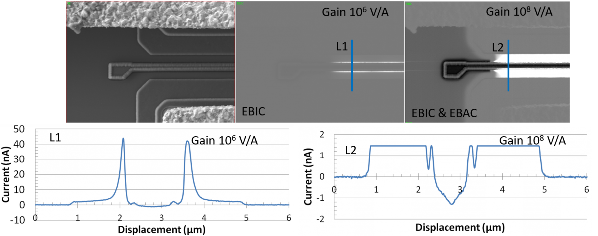
P-N junction in microchip, the low gain image shows the properties of the junction while the high gain image starts to visualise the connections in the chip.
EBAC is a measure of electrons from the electron beam which are absorbed into the sample and flow to the probe. A common application is to locate failures in circuitry such as shorts or open circuits. The example below shows a cracked microchip, at the crack it is clear the EBAC signal terminates. While the failure is obvious, this method can be used to analyse buried failures that are not visible in the imaging. It is worth noting that this is the same microchip from the above EBIC example, but the accelerating voltage is reduced so the P-N junctions are not activated.
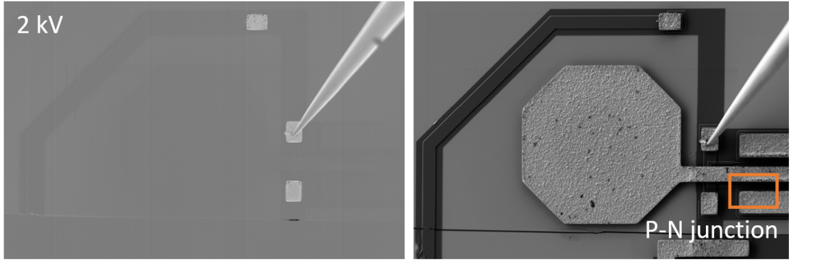
EBAC image of a microchip, clear that the crack is preventing any current flowing to the probe. The orange box indicates the region imaged in the previous EBIC image.
Both EBIC and EBAC measure electrons from the sample flowing through to the probe, and are consequently dependant on the precise contact point of the probe on the sample. More complex applications use multiple probes to measure flow relative to set points or bias the sample to active certain devices and change the flow.
Hopefully this very brief introduction will give you an idea on what type of electrical testing can be carried out in electron microscopes. To find out more about electrical testing with OmniProbe see our application note: Multi-Scale Analysis of Dislocations and Grain Boundaries for Improving mc-Si Solar Cell Performance.