1st September 2021 | Author: Dr Pat Trimby
Is large area TKD really possible?
This week, I was reading through a draft manuscript presenting the use of large area EBSD mapping to characterise the microstructures in a suite of Martian meteorites from which we can learn a lot about the conditions (pressure, temperature, strain rate) under which they were deformed. It was interesting work and demonstrated very clearly the power of combining SEM stage movements with high-speed EBSD mapping in order to cover large areas on the surface of our samples. In a recent post, Kim Larsen gave some great tips and tricks on how to use the Large Area Mapping functionality in AZtec to do this, but here I want to focus on something that might sound similar but is in fact totally different.
Large area TKD
Transmission Kikuchi Diffraction (TKD) is essentially the analysis of electron transparent samples using a conventional EBSD system and was the subject of a post I wrote earlier in the year.
TKD enables significantly improved spatial resolution compared to conventional EBSD but, like conventional transmission electron microscopy (TEM), the areas analysed can be extremely small and therefore are perhaps not representative of the whole sample. The size of the electron-transparent area will be completely dependent on the sample preparation technique.
Preparing metals and alloys
For many metals and alloys, we can use electropolishing of standard 3 mm diameter TEM discs; although this is not really a site-specific approach (i.e. it is hard to target particular features or regions in our sample), it does usually provide a relatively large, thin area around the edge of the central perforation.
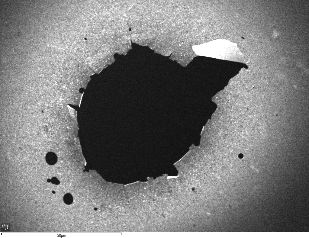
This is clear in the secondary electron (SE) image from an electropolished Al-alloy shown below; the brighter ring around the perforation is the electron transparent area (where SEs are escaping from both the upper and the lower surfaces of the sample), and the darker area directly adjacent to the perforation is the really thin part of the sample (where most electrons are transmitted without interacting with the sample, and hence the SE yield is lower). It is usually this darker area that is ideal for the highest resolution TKD (and also high resolution TEM).

SE image of an electropolished TEM disc from a highly deformed, nanocrystalline Al-alloy, showing the brighter electron-transparent region around the central perforation.
If we use a sensitive, high-speed EBSD detector such as our Symmetry S2, then we can survey, at relatively low magnification, the microstructure all the way around the perforation. At this magnification, we are not normally too focused on the best spatial resolution and therefore can use a higher beam current to increase speed.
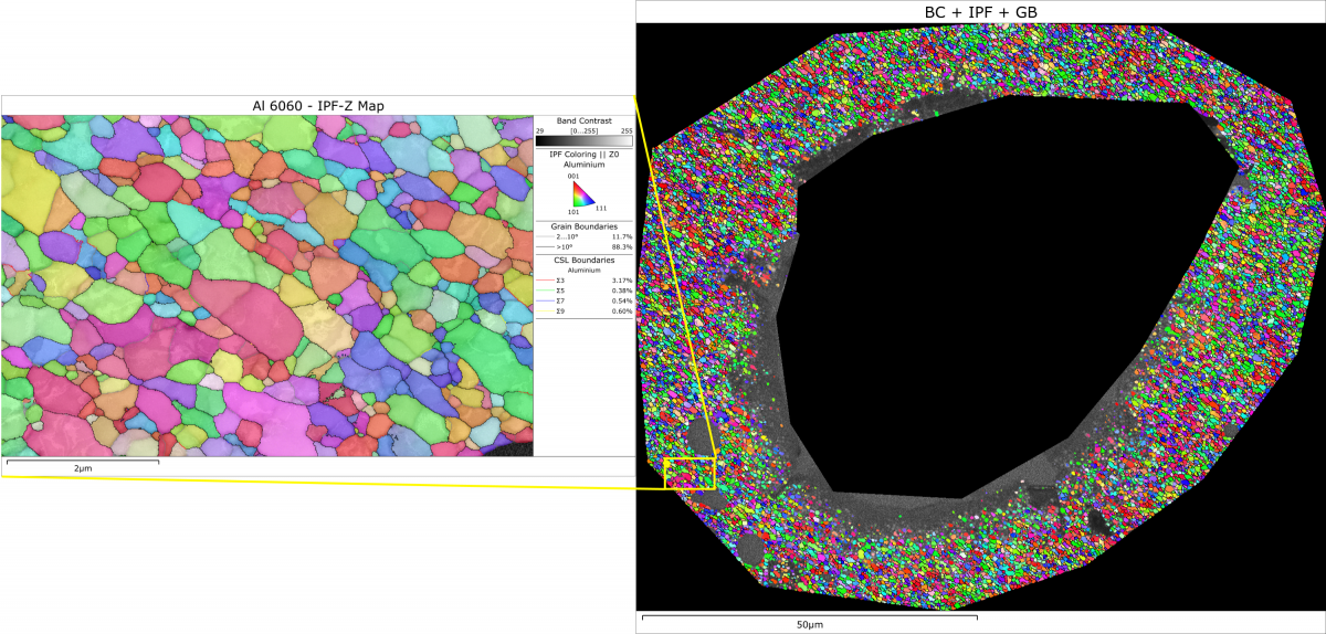
The following image shows an orientation map (on the right) that was collected from the same sample as shown in the SE image above, analysed at over 700 patterns per second with a measurement step size of about 60 nm. The whole scan took just over 20 minutes; this allows us to find regions of interest that we can then analyse at higher magnification using a lower beam current (for higher resolution), as shown on the left-hand map (analysed at 125 pps, with a 10 nm step size).

TKD orientation maps of a severely deformed Al-alloy. The right-hand survey scan was collected at >700 pps in about 20 minutes (scale bar 50 um), enabling higher-resolution analyses of specific regions of interest, as shown on the left (scale bar 2 um).
Preparing non-metallic materials
Preparing non-metallic materials or site-specific samples for TKD analyses will almost always involve the use of a focused ion beam (FIB) SEM. The development of these instruments over the past 2 decades has been astounding, and it is now a routine procedure to work through the steps required to prepare a high-quality lift-out sample for either TKD or TEM analysis.
However, FIB-prepared samples are usually fairly limited in size (e.g. typically 20 x 10 um) and, for surface films, it is very challenging to prepare plan-view samples (as opposed to a cross section through the surface film). In response to this, we have been developing a new approach to TKD sample preparation at Oxford Instruments that enables rapid preparation of plan view samples (ideal for thin film TKD) and offers significant potential for large area TKD sample preparation.
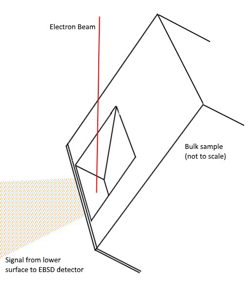
The approach is simple and utilises the fact that for TKD we often tilt the sample slightly away from the side-mounted EBSD detector. This means that we can mill, using the FIB beam, on the side of a bulk sample and effectively prepare an electron transparent sample without ever needing to mill the sample surface of interest. Assuming that the EBSD detector is mounted on the FIB-SEM, it is then simply a matter of tilting the sample by another 10-20° from the milling geometry to position it in the ideal position for TKD, as shown below.

Schematic illustration showing the geometry for TKD following a new, fast sample-preparation technique, ideal for the analysis of surface thin films. The thin film is positioned on the lower surface of the image in this set-up.
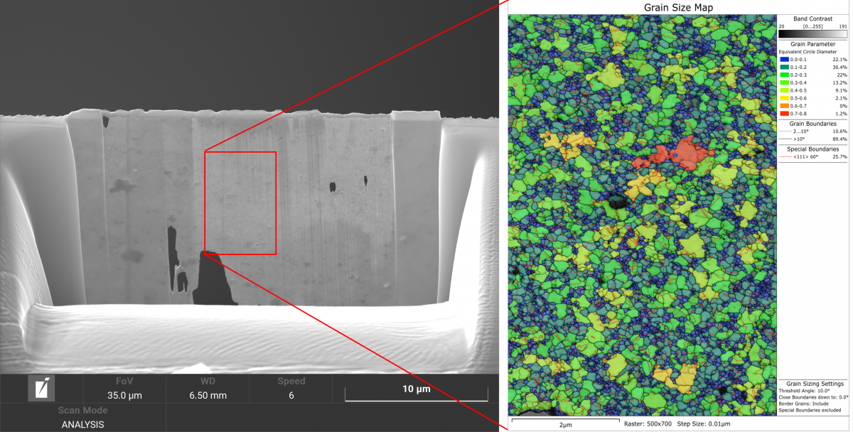
As an example of how well this approach works, we prepared a plan-view TKD sample from a 200 nm thick nanocrystalline Au thin film on a Si substrate. From start to finish, the preparation took about 25 minutes, with no requirement for lift-out and no exposure of the surface film to the ion beam. The resulting TKD grain size map is shown in the following image.

SE image showing the final prepared TKD sample of a 200 nm thick Au film, along with a grain size map from the subsequent TKD analysis.
This approach holds a lot of potential for a wide range of sample types, but there is one possible application that really excites me. Increasingly, we see FIB-SEMs with plasma ion sources and, in some cases, equipped with femtosecond (fs) lasers. These offer the potential to mill away extremely large volumes of material in a very short time period.
Given that this new sample preparation technique involves no lift-out, we can start to prepare extremely large area, electron transparent samples using plasma FIBs or fs lasers. Both beams have been shown to produce minimal damage to the crystal structure (especially when compared to Ga ion beams), and we have already managed to prepare TKD samples > 200 um across and to collect “large area” TKD maps.
The exciting part for me is that, with these new fast milling techniques, the sample preparation time remains just a matter of minutes, leaving more time to analyse your sample and to focus on the microstructural problems that we want to solve.
So, next time you are facing up to the challenges of preparing a plan-view TKD sample or want to try and perform a large area TKD analysis, give this technique a go!


