Elemental and Structural Characterisation of Semiconductor Devices

As the complexity of devices increases, no matter what their function, the value of single wafers increases. As this value increases, it becomes less desirable to break a wafer to perform physical analysis tasks. This increases the demand to perform elemental characterisation on bulk specimens. One of the best ways to achieve spatially resolved elemental characterisation is using the scanning electron microscope and EDS. The challenge for characterisation in SEM, or indeed a focused ion beam (FIB), is that although most of the nanometre scale features can be imaged using low kV electrons, elemental analysis at this resolution and under these conditions is not typically possible.
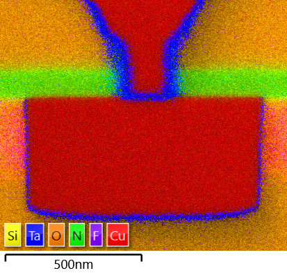
Ultim Max Extreme can solve this problem. The optimisation of the Extreme detector to allow high X-ray collection efficiency at the conditions required for Ultra high-resolution image and the powerful x-ray spectrum processing supplied by AZtec make 5nm resolution EDS on bulk samples a possibility. Achieving elemental characterisation at this resolution reduces the requirement for thin specimens and transmission electron microscopy (TEM) decreasing time to data and improving productivity.
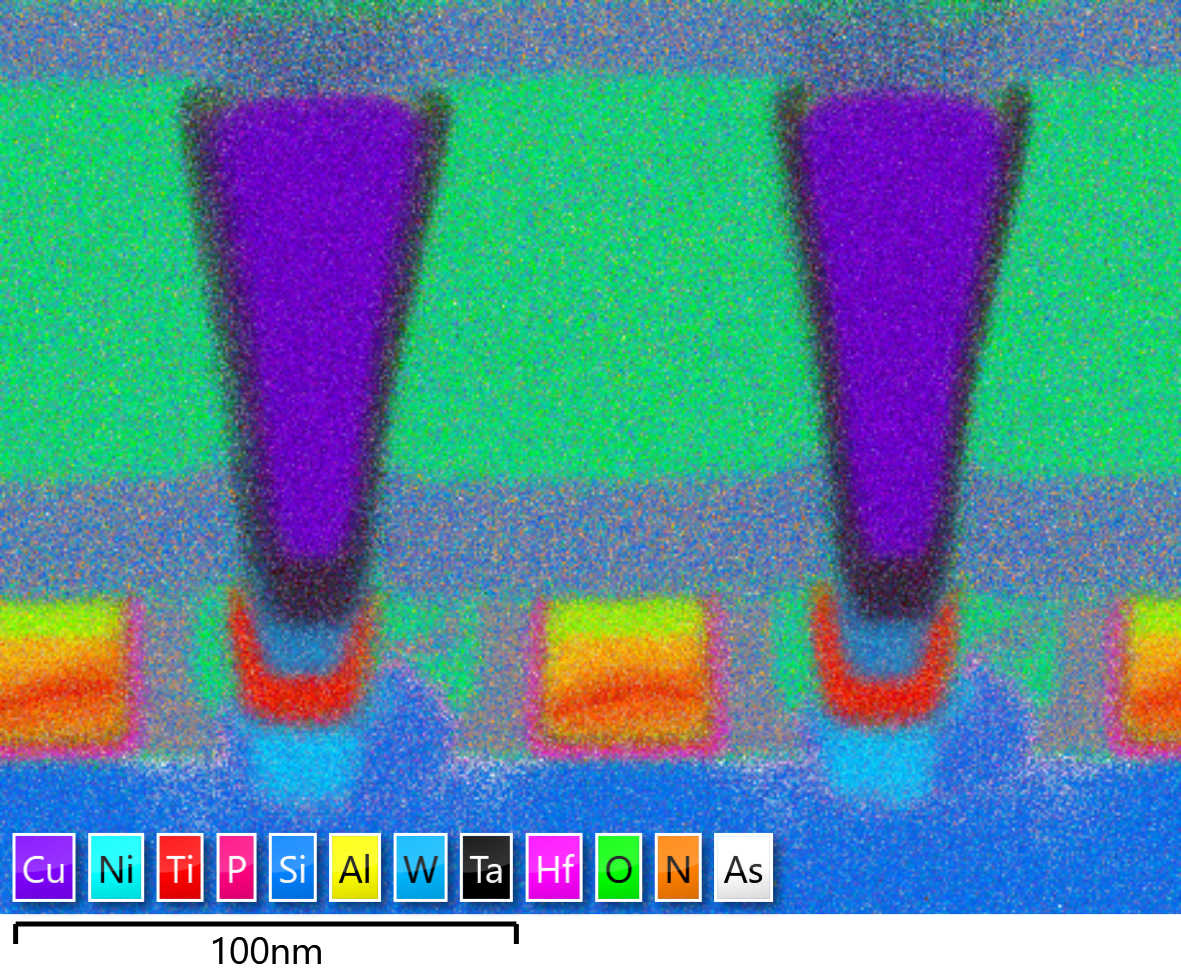
However, for some specimens, the resolution requirements still require electron transparent specimens to be prepared. Whether this is characterising the uniformity of a gate oxide layer, the integrity of a diffusion barrier at a metal-semiconductor interface or the distribution of dopants in a PN junction. Some of this work can still be performed using transmission mode imaging in the FIB during sample preparation where due to the extreme sensitivity Ultim Extreme is still the detector of choice. Most of this work does, however, require TEM where angstrom resolution imaging and elemental analysis is routinely performed. Our flagship detector for TEM, Ultim Max TLE, is the optimum solution. An optimised sensor design ensures maximum sensitivity whilst the windowless nature of the detector ensures improved sensitivity for light elements such Boron which is often used for p and n type doping in semiconductor devices.
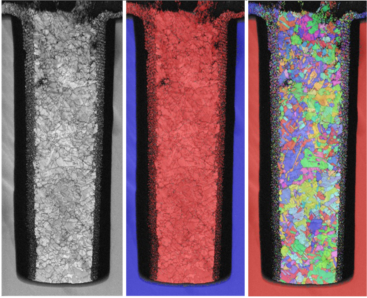
It is not only the elemental properties of the materials that can strongly affect the performance of a device. The crystal structure, grain structure and strains within metallised features can strongly affect the electrical conductivity and even susceptibility to oxidation. Whether the feature is a front end interconnect, through silicon via (TSV) or back-end bond pad understanding the structure can be key to understanding device performance. EBSD gives spatially resolved structural information by mapping the change in electron diffraction from a specimen surface. Comparatively large features such as TSVs can have their electrical transport properties defined by nanometre scale grains. Symmetry EBSD solves these problems. Being the world first CMOS based EBSD camera means that it can achieve speeds 10x faster than a conventional CCD based EBSD camera on the same materials. This means that high-resolution EBSD maps can be collected much faster. Therefore small grains can be analysed over large areas.
Not all analysis requires high-resolution elemental analysis. In a lot of situations, it is much more important to have high throughput and interactive feedback in understanding the elemental distribution of a sample. One example of this would be when analysing the formation of intermetallic contact layers at solder joints. With a large array of solder joints being able to quickly identify the joints with a large diffusion of copper bond pad into tin solder is usually left to backscattered electron (BSE) imaging. Using AZtecLive it is now possible to perform the same task using the combination BSE and EDS this adds an extra layer of information to truly understand the process that leads to this intermetallic formation.
Back to Semiconductors, Microelectronics & Data Storage