Part of the Oxford Instruments Group
Expand

Ultim® Extreme

Ultimate spatial resolution and low energy performance for EDS in the SEM. Combining Extreme electronics and windowless construction with optimised geometry and sensor design delivers up to 15x greater sensitivity than a conventional large area SDD.

  • Optimised for analysis under the most demanding conditions

  • Work at energies of less than 2kV for sub 10nm spatial resolution

  • Take advantage of surface sensitivity to replace expensive surface science tools

  • High sensitivity for light elements such as nitrogen and oxygen

  • Combine with immersion optics to collect high sensitivity data at up to 30kV


Request Pricing Add to quote list

Ultim Extreme Silicon Drift Detector is a breakthrough solution for ultra high resolution FEG-SEM applications and delivers solutions beyond conventional micro- and nano-analysis.

The Ultim Extreme is a windowless 100 mm2 version of Ultim designed to maximise sensitivity and spatial resolution. It uses a radical geometry to optimise both imaging and EDS performance in ultra-high resolution FEG-SEMs while working at low kV and short working distance. With Ultim Extreme, EDS resolution approaches that of the SEM.

  • Ultimate spatial resolution for SEM-EDS
    • Sub 10nm element characterisation in the FEG-SEM

  • Surface science sensitivity
    • Characterise surfaces in the SEM

  • Materials discrimination at the lowest kV
    • Down to 1kV materials characterisation

  • Fastest and most accurate nano-characterisation
    • Fast collection, real-time data processing from a bulk sample
  • Extreme light element sensitivity
    • New levels of detectability for elements such as lithium, nitrogen and oxygen
Discover Solutions for Biological Science Discover Solutions for Material Science

Solutions for Material Science

Ultim Extreme a breakthrough solution for ultra high resolution FEG-SEM. This unique detector for the first time enables EDS data collection at very low kV (e.g. 1-3kV) and very short working distance to provide elemental analysis under the conditions customers are using to analyse nano-materials and surfaces at the highest SEM resolution.

The latest ultra-high resolution FEG-SEMs offer new capabilities for investigating smaller nano-structures, interfaces and surfaces. However, under the conditions used, with very short working distance, very low kV and minimal beam current, to make use of new electron signal contrasts from in-lens detectors, no current EDS can provide supporting elemental characterisation. Ultim Extreme changes this, it was designed specifically to operate in this analysis regime with:

  • Unique geometry
    • Designed to work at a shorter working distance
    • Designed with the highest solid angle for a conventional port mounted EDS detector – typically 5x greater solid angle than Ultim Max 170, with the sensor half the normal distance to the sample

  • Windowless operation
    • In combination with the solid angle 10-30x higher sensitivity for low energy X-rays compared to any other large area detectors
  • New detector electronics for boosted sensitivity to very low energy X-rays and extended low energy analytical performance at higher count rates
  • Integration with AZtecLive and its Tru-Q® analysis engine for low kV data processing and analysis
    •  TruMap optimisation for low kV overlap correction

To achieve this unique geometry, the Ultim Extreme is designed with the non-circular 100 mm2 sensor and windowless configuration already successfully used in the X-MaxN 100TLE to optimise sensitivity in the TEM. In addition the detector features a new reduced footprint electron trap configuration to allow accurate quantitative analysis up to 7kV beam voltage with qualitative elemental analysis at higher energies.

  • Sub 10nm element characterisation in the SEM
  • X-ray map resolution close to SEM resolution

Example 1: Semiconductor device

X-ray map of smartphone CPU acquired at 3kV. 38,000cps for 30 minutes - sample and data courtesy of MSSCorps.

Example 2: Sn imaging standard

X-ray mapping at 2kV of tin nano-sphere high resolution imaging standard, 6,500cps, 15 min acquisition time.

Example 3: Ni-base Superalloy

Fine Ni3(NbTi) gamma” precipitates in Alloy 718, collected at 1.5 kV, 2,000cps for 18 minutes - Sample and data courtesy of University of Manchester.

With Ultim Extreme users can characterise the composition and distribution of surface contaminants and layers a few atoms thick.

  • Integrate characterisation of surfaces with SEM investigation
  • Analyse the surface structures only visible with in-lens detectors at very low kV and short working distance
  • Save money and time vs Auger/XPS

Example: X-ray Maps collected at 1kV to characterise high-end electronic component stain detected using In Lens SE imaging.

Materials characterisation at 2kV or less

  • Fully integrate EDS where very low kV electron microscopy benefits sample characterisation
    • For enhanced signal contrast
    • Reduction of sample damage e.g for polymers and soft coatings
    • Reduce charging or achieving charge balance conditions


Example: Reducing accelerating voltage from 10 to 1.5kV allows electron image contrast to show the distribution of oxide particles. X-ray mapping under the same conditions characterises precipitates as MnOB. Map acquisition time 15 minutes. Sample courtesy of JFE Steel.

 Fastest nano-characterisation

  • High speed collection
  • Real- time data processing of low kV spectral data
  • Bulk sample – simple sample preparation

Example: X-ray QuantMaps collected at 3kV, 15,000cps for 22 minutes to characterise NbTi Nitride and Al Oxide nano-precipitates in a Ni- base superalloy (Alloy 718). Sample and data courtesy of University of Manchester.

Most accurate nano-characterisation

  • Real-time data processing
  • Unrivalled low energy spectrum quality and integrity
  • Rapid automatic element identification
  • Peak overlap correction of low energy X-ray line series

Example: Spectrum processing of low energy lines to create QuantMaps to characterise NbTi Nitride and Al Oxide nano-precipitates in a Ni- base superalloy (Alloy 718)

Ultim Extreme uses a special electron trap and windowless operation to achieve the required performance to meet its target applications. Its windowless operation provides improvements in count rate of 2-3x for light elements, and nearly 1.5x for the highest lines that can be detected. In combination with the improvement in solid angle this provides a sensitivity boost of 10-30x compared to conventional large area SDD with thin windows. For extremely low energy lines the improvements is even greater and further increased by the use of extreme electronics developed for Li-detection.

  • Windowless configuration offers the most sensitive light element detection
    • Up to 3x increase in signal over conventional SDD detectors
    • New potential for the detection of difficult elements such as nitrogen

Example: First detection of Lithium


Solutions for Biological Samples

Ultim Extreme provides definitive elemental detection for biological samples, enabling fast, accurate data collection in low kV conditions suited to life science SEM applications. A very short working distance and windowless award-winning detector design combined with our optimised electronics and data processing results in 10-30x higher sensitivity for low energy X-rays.

The Ultim Extreme detector for biological applications demonstrates:

100nm section of unstained leaf tissue on aluminium stub, imaged using 2.5kV for 15 minutes.

100nm section of unstained leaf tissue on aluminium stub, imaged using 2.5kV for 15 minutes. 

Venus’ fly trap leaves and glands imaged with the Ultim Extreme detector at 5kV

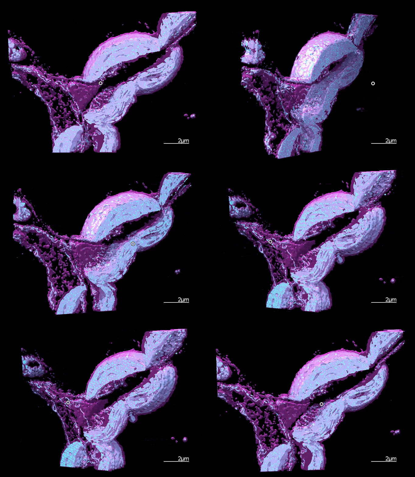
Venus’ fly trap leaves and glands imaged with the Ultim Extreme detector at 5kV. Layered EDS maps shows clear nitrogen signals as well as a differential osmium and zinc localisation (left). Osmium can be used as a mask when applied to backscattered images collected across several sections using array tomography (yellow in middle image and pink in right image showing 3D data of chloroplasts).

Learn more on EDS for Biology

Learning centre

High-resolution materials characterisation

This webinar will identify the challenges, and provide information on optimising microscope conditions to maximise results, demonstrating the strengths of combining high-resolution SEM with windowless EDS analysis to enable nanometre chemical analysis of key material features.

Watch now
How Live Chemical Imaging can Help Biologists Find Rare Events

Discover how Live Chemical Imaging is a powerful tool for electron microscopists and can significantly speed up any investigation by combining ultrastructural information from the electron images with compositional information from EDS.

Download
EDS Characterization of the SRAM device

This application note shows how devices must be characterised to ensure that they have been manufactured correctly and to investigate any failures to achieve the necessary performance.

Download
Photomask Inspection with SEM-EDS - A Critical Part of the Semiconductor Manufacturing Process

This application note will be inspecting photomask quality in terms of defects and cleanliness – including those defects that cannot be identified using optical methods, using Oxford Instruments' Ultim Extreme detector.

Download
Mapping Semiconductor Devices in the SEM

That by using low kV SEM to analyse semiconductor materials, it can reveal information that would otherwise be indiscernible at higher kV.


Download
Analysing a NAND Flash memory device using low kV EDS

Discover how to accurately map the elemental distributions in
complex specimens with nano-structures such as a NAND flash memory device.

Download
Quantifying Metal Cleanliness - boride and nitride non-metallic inclusions

Find out how the flexibility of a more conventional setup with the ability to detect light elements and minor constituents during automated particle analysis runs and, the acquisition of very high resolution EDS maps.


Download
Nanocolumn Gallium Nitride (GaN) growth control inspection

Checking the quality of Metalorganic vapour-phase epitaxy (MOVPE) overgrowth above an array of GaN nanotubes. Discover how GaN samples containing a high density of nano-columns can be quickly and non-destructively analysed using an Ultim Extreme EDS detector.

Download
Ultim Extreme

The Ultim Extreme is a windowless 100 mm2 version of Ultim designed to maximise sensitivity and spatial resolution. It uses a radical geometry to optimise both imaging and EDS performance in ultra-high resolution FEG-SEMs.

Download
How to analyse nanoparticles using EDS in the SEM

Discover how with the latest hardware and software development in the EDS technique and the improvement in high-resolution SEM performance at low kV, It is possible to perform low kV EDS analysis with high quality on studying nanoparticles.

Download