Part of the Oxford Instruments Group
Expand
Semiconductors, Microelectronics & Data Storage
Fault Identification and Isolation

Understanding the root cause of failures that affect yield, performance or reliability of device is critical to the semiconductor manufacturing process. As devices shrink and geometries become ever more complex it becomes increasing difficult to find subtle electrical defects and isolate them from the devices as a whole.

Fault Identification and Isolation

One of the big challenges in semiconductor failure analysis is finding the actual failed device. Optical techniques such as optical beam induced resistance change (OBIRCH) give a general area but typically do not have single device resolution. Even in an SEM, the failure site may not actually be visible due to it being located in a buried layer. For these nanometre scale devices electron beam induced current (EBIC) and electron beam absorbed current (EBAC) imaging allow visualisation and mapping of the electrical response of a device, even for sub surface structures. The reproducible nanoscale positioning achieved by omniprobe 200 and 400 allow electrical contact to be made with the smallest device features. This allows electrical testing of current generation IC devices. 

Once a failed device is located it is usually necessary to isolate or remove it for further physical analysis. This is usually achieved via a lift out process to access buried devices and allow investigation at high resolution using TEM. As devices become smaller this becomes more difficult the lift out must be on the length scale of that device and more site specific to reduce impact on the rest of the processed wafer.  These challenges must be overcome whilst still meeting the demanding throughput requirements of the failure analysis industry. OP400 provides a solution to many of these challenges. The piezo driven motion allow positioning accuracy to 25 nm allowing site specificity on the smallest feature. This small step size also means fluid movement in the electron image allowing users to position the probe quickly with repeatability thus decreasing the time to lift out. Productivity is further enhanced by in-situ tip exchange which decreases down time in the event of a tip crash. 

Finally, with rotation as standard on the OP400 a huge array of sample geometries can be achieved enabling advanced preparation techniques such as back-side-thinning. Techniques like this reduce the effect of curtaining in a sample thus allowing higher resolution analysis when a sample finally makes it to the TEM. To ensure optimised lamellae preparation OmniProbe can be used in tandem with EDS and AZtec LayerProbe to deliver feedback on specimen thickness and contamination induced by the fabrication ion beam.

Back to Semiconductors, Microelectronics & Data Storage

Application Notes

High quality TEM lamella preparation and on-tip analysis using LayerProbe and the OmniProbe 400

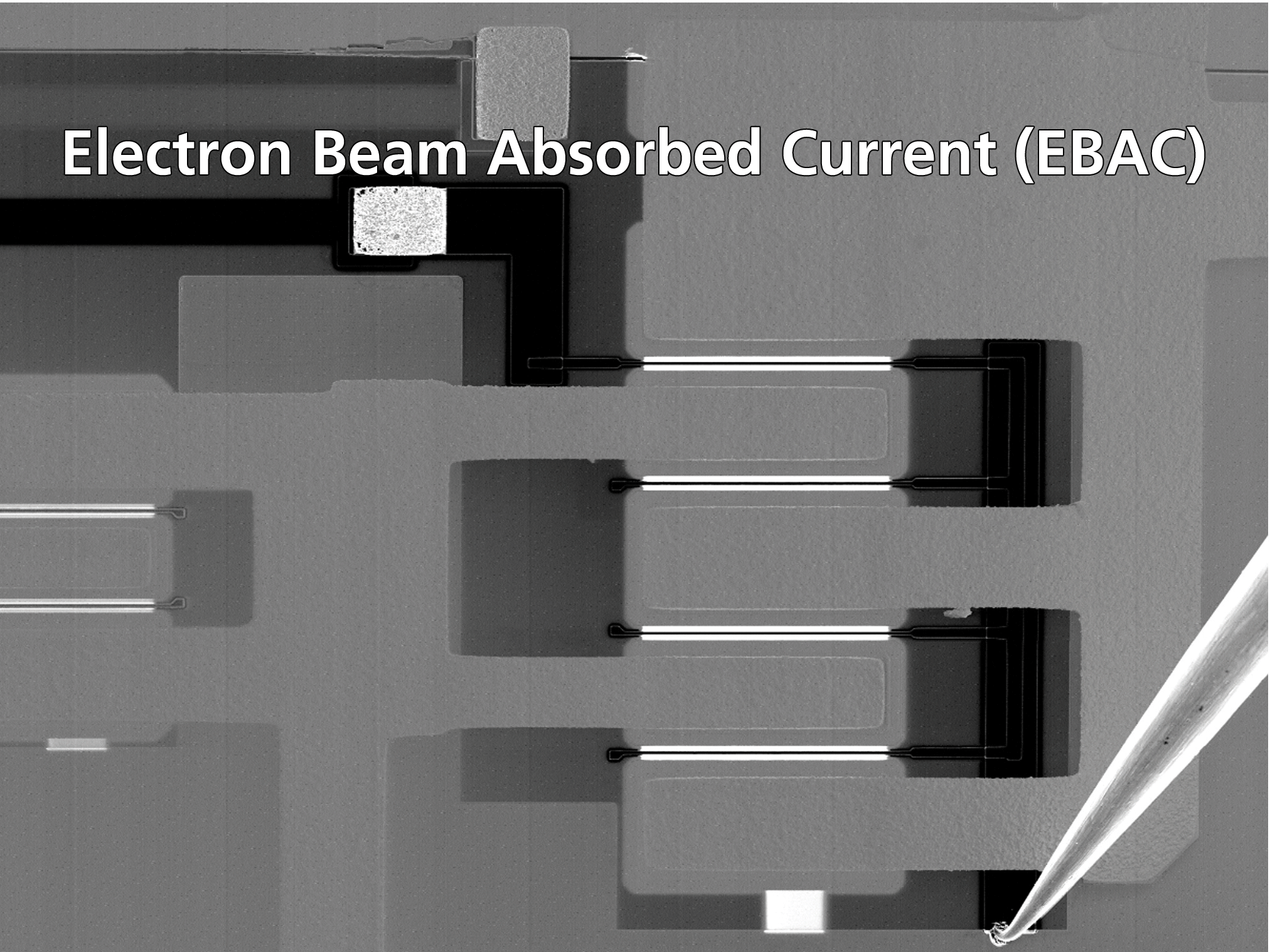
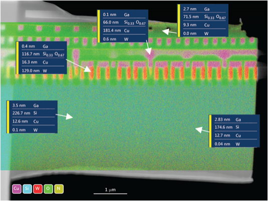
Here we present a new technique that enables measurement of the local thickness and composition of TEM lamellae and discuss its application to the failure analysis of semiconductor devices.

Download

Related Products

Get in touch with one of our Application Specialists...