12th May 2021 | Author: Dr Haithem Mansour
The importance of hardware components for EDS: the sensor
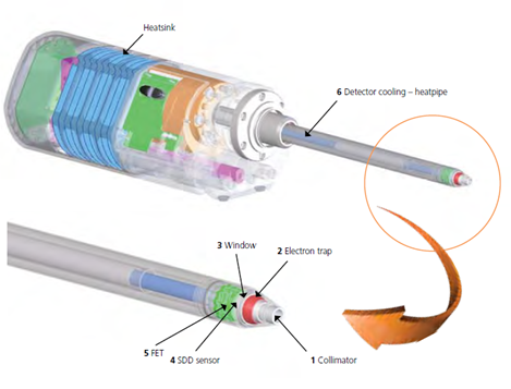
This blog post is the second part of the “Importance of hardware components for EDS” series. In the previous post, I highlighted the importance of the collimator assembly, the electron trap and the window in delivering fast, accurate and reliable EDS data.
This time, I will continue with a key component, perhaps the most important one in an EDS detector: the sensor.
The EDS sensor is a semiconductor device that, through the process of ionisation, converts an X-ray of a particular energy into an electric charge of proportional size.
Types of EDS sensor
There are two types of sensor used for EDS: SDD and Si(Li). Traditional silicon crystals drifted with lithium, so called “Si(Li)”, were first commercialised in the late 1960s. The Si(Li) requires very low operating temperature (90°K) to separate charge signals from electronic noise and is normally cooled using a reservoir of liquid nitrogen. The second type is the Silicon Drift Detector (known as SDD). The SDD has completely replaced the Si(Li) technology due to superior performance. It is much faster, has better resolution (especially as count rates increase), and only requires cooling to a few tens of degrees below zero.

Fig.1. Cutaway diagram showing construction of an EDS SDD detector
What role is played by the SDD in an EDS detector?
The EDS detector converts the energy of each individual X-ray into a voltage signal of proportional size. This is achieved through different stages. The SDD is responsible for the first stage, which is the conversion of X-ray into charge by ionisation of atoms in the semiconductor crystal.
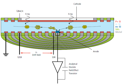
When an incident X-ray hits the SDD, its energy is absorbed by a series of ionisations within the semiconductor to create several electron-hole pairs (Fig.3). The electrons are then raised to the conductive band of the SDD and are free to move within the crystal lattice. When an electron is raised to the conductive band, it leaves a “hole” behind which behaves like a free positive charge in the crystal. A bias voltage applied across the SDD “drifts” the electrons down a field gradient between the drift rings. The electrons are then collected at the anode. This design means the anode size can be kept to a minimum, reducing the sensor circuit capacitance and therefore the voltage noise of the detector. With lower noise, the amount of time required to process the signal is lower, and a higher number of X-rays can be counted more accurately. This means good spectral resolution can be achieved at high count rate, a key strength of SDD technology.

Fig.2. Construction and operation of an SDD detector
Size of an SDD
EDS detectors comes with different SDD sensor sizes, e.g. for the Ultim Max range, it is available with 40mm2, 65mm2, 100mm2 or 170mm2 sensors. The larger the sensor size, the larger the surface of detection and the higher number of X-rays detected (input count rate). Fig.3 highlights the difference in counts per second between different SDD sizes under the same experimental conditions.
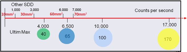
Fig.3. Counts per second vs SDD sensor size
It is a challenge to maintain high performance of large sensors sizes . For example, detectors with large sensors require higher power to cool to the same temperature. The environmental, cooling technology and engineering challenges are significant if the detector current noise, which also influences the resolution, is to be kept to a minimum and stable over time. Using the same small anode on all sensor sizes is important to ensure large area SDD sensors can maintain good resolution at very high-count rates, which they can more easily achieve due to their size.
It is important to keep detector resolution on the largest sensors as high as can be achieved by the smallest sensors. This is because large area detectors are used for low-kV nanoanalysis, where peaks are poorly separated and spectral resolution is at its most important. Oxford Instruments tests all its Ultim detectors for low energy resolution using C K X-rays, during detector manufacture and installation, to ensure high performance is achieved for all sensor sizes.
Hopefully, this has given an overview of the importance of the SDD and the role that this component plays to deliver accurate and fast EDS data. In my next post, I will continue with the FET and cooling system.