31st March 2021 | Author: Dr Sam Marks
Introduction to EDS for Semiconductor analysis
Moore’s law states that every two years the number of transistors within an integrated circuit doubles. This observation has been driving the semiconductor industry for nearly 50 years, as they strive for smaller semiconductor devices that can be fabricated within the same amount of space. A remarkable feat of modern era technological advancement, we have seen MOSFET nodes reduce in size from 10 µm in the 1970’s to 5 nm in 2020. As semiconductor devices utilise electron transport through a range of different materials, it is crucial to be able to quantify what elements are present within a semiconductor device and to acquire spectral images of those elements to measure critical thickness values.

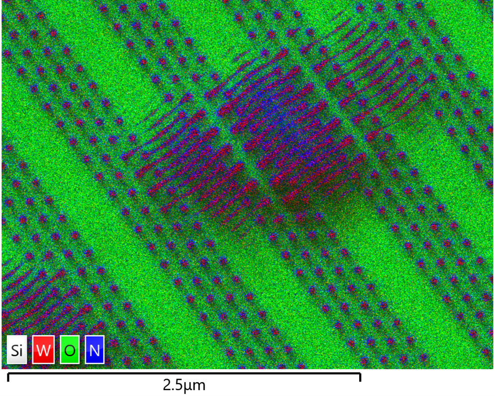
De-layered NAND device acquired in the SEM at 3 kV.
These measurements are performed using either a Scanning Electron Microscope (SEM) or a Transmission Electron Microscope (TEM) dependant on feature size and the level of analysis required. Energy Dispersive Spectroscopy (EDS) is an integral part of this analysis, as it allows users to characterise the materials, measure the thicknesses of the material layers and identify any erroneous material. EDS analysis can generalise samples to three categories bulk SEM, STEM-SEM and S/TEM.
Bulk SEM
Bulk SEM analysis examines either a full sample or a fraction of a whole sample, for example a cross section of a wafer. As component sizes have decreased, we have seen a rise in low kV EDS analysis, as this allows users to optimise the spatial resolution of both their microscope and their EDS maps. For these samples we recommend the Ultim® Extreme detector, as this detector has been optimised to operate at short working distances, allowing users to achieve a greater spatial resolution without sacrificing their X-ray count rate. The main limitation of bulk SEM analysis is the spatial resolution which is typically limited to features > 10 nm, a result of the X-ray interaction volume in a bulk material.

3 kV EDS mapping of a bulk de-layered NAND device using Ultim Extreme. 20 nm features can clearly be seen in the EDS maps and successful peak deconvolution between Si and W is observed.
STEM-SEM
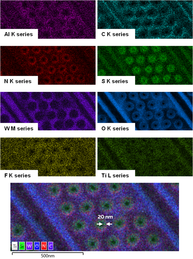
STEM-SEM analysis is an intermediary technique that is seeing a resurgence in popularity due to improvements in SEM technologies, ease of use and time to acquisition. STEM-SEM requires electron transparent samples, typically ≤ 100 nm thick, the same samples that can be analysed using TEM. The most common sample preparation approach is to perform a FIB-SEM liftout, targeting a region of interest and thinning to electron transparency with the FIB. Once the sample is prepared it is loaded into a STEM sample holder and placed back into a FIB-SEM or SEM with STEM capabilities. Spectral imaging spatial resolution is significantly improved for STEM-SEM, allowing mapping of features ≥ 5 nm, as the microscope can be operated at higher accelerating voltages, typically 30 kV, and the electron transparent property of the sample removes resolution loss due to interaction volume. Both Ultim® Extreme and Ultim® Max 170 provide strong analytic solutions when paired to STEM-SEM systems.
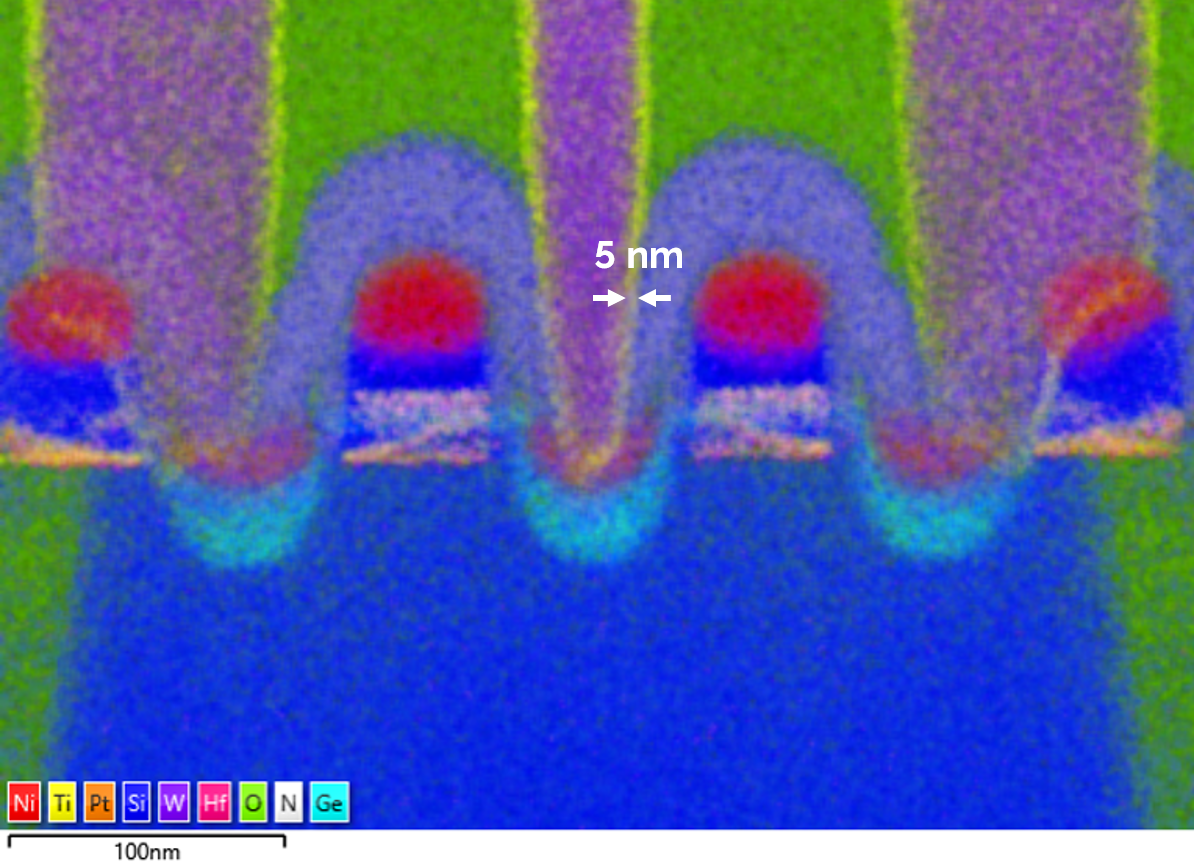
Example QuantMap of a semiconductor device cross section in TEM. The complexity of semiconductor devices is observed here with 11 elements present, mapped and peak deconvoluted.
TEM
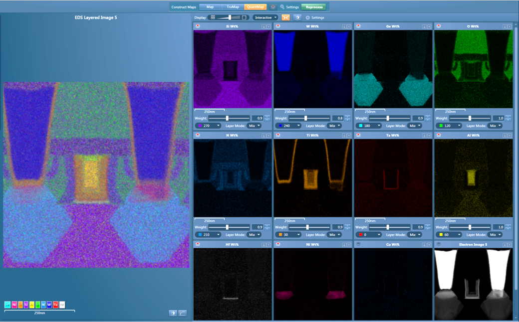
TEM is the ultimate analytical instrument in terms of magnification, capable of atomic resolution spectral imaging. However, it is often the most time-consuming and complex analytical process requiring advanced sample preparation routines and significant microscope beam alignments. TEM requires an electron transparent sample, < 100 nm thick, with maximum sample size being a 3 mm diameter disc. TEM plays a key role in semiconductor research and development where it provides high resolution images and EDS maps to identify exact chemical compositions and critical dimensions. The Ultim Max TLE detector is optimised for this application, achieving the maximum solid angle available per microscope, is windowless for enhanced light element sensitivity and has an enhanced TEM quantification routine, known as M2T, allowing for enhanced absorption corrected quantification and sample thickness measurements.
Example QuantMap of a semiconductor device cross section in TEM. The complexity of semiconductor devices is observed here with 11 elements present, mapped and peak deconvoluted.
As we drive towards sub < 5 nm semiconductor devices, the margin for error in these devices reduces increasing the need for high resolution electron microscopy and EDS. This blog post has explained the basic difference between the three main EDS analysis types. To learn more about EDS and Semiconductor applications, visit our application library or access some of the resources listed below.