In 25 years at Oxford Instruments, I have been lucky enough to be at the centre of a number of advancements in the capability of elemental analysis using SEM-EDS. Two big ones spring to mind:
- The massive improvement of spatial resolution allowing routine characterisation of nano-structures using low kV FEG-SEM and large area SDD like Ultim Max or special detectors like Ultim Extreme for those really small, sub-20 nm features.
- The step change in accuracy and reliability of the standardless quantitative analysis of micro-structures at high kV where better than +/-2% is achievable with Tru-Q technology and the best practice collection methods we outlined in our webinar on quantitative analysis last year.
An outstanding question which has proved more complicated to answer is how to quantify nano-structures with the same kind of accuracy that we can achieve on micro-structures at high kV? There are many additional challenges with low-kV data collection and quantification, something that could fill a blog or two just on its own. One challenge, which fills the contents of many papers and sessions at conferences, is the problem of quantifying low energy X-ray lines due to uncertainties in X-ray emission caused by the involvement of valence electrons in their formation, and the much greater levels of interaction with the sample making matrix corrections more difficult.
As part of our studies into these challenges, we are also starting to consider in greater depth the potential capability of a different method that allows us to use high-kV for quantitative analysis on nano-structures. This is done by analysing a thin lamella rather than a bulk sample, so called SEM-STEM or 30kV STEM. It’s a somewhat mis-leading term, as a STEM detector is not a requirement, but it takes advantage of the much smaller volume of interaction when an electron beam interacts with a thin sample / lamella at high kV. I attempt to show this using simulations of sample – beam interaction in Figure 1.

Figure 1. X-ray generation of Mn X-rays in MnS from a bulk material at 20kV (left), a 250nm thick lamella at 30kV (middle) and a 100nm thick lamella at 30kV (right) determined by Monte Carlo simulation.
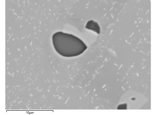
One sample we have been looking at is a steel with a range of inclusions of different sizes (Fig. 2). We are interested in this sample because it has large inclusions with a size range of 2-10 µm. The composition of these inclusions can be determined using conventional SEM-EDS, and then re-measured from a thin lamella cut from the sample using a FIB.
Figure 2. BSE image of a steel sample with inclusions with sizes ranging from 100nm to >5 µm
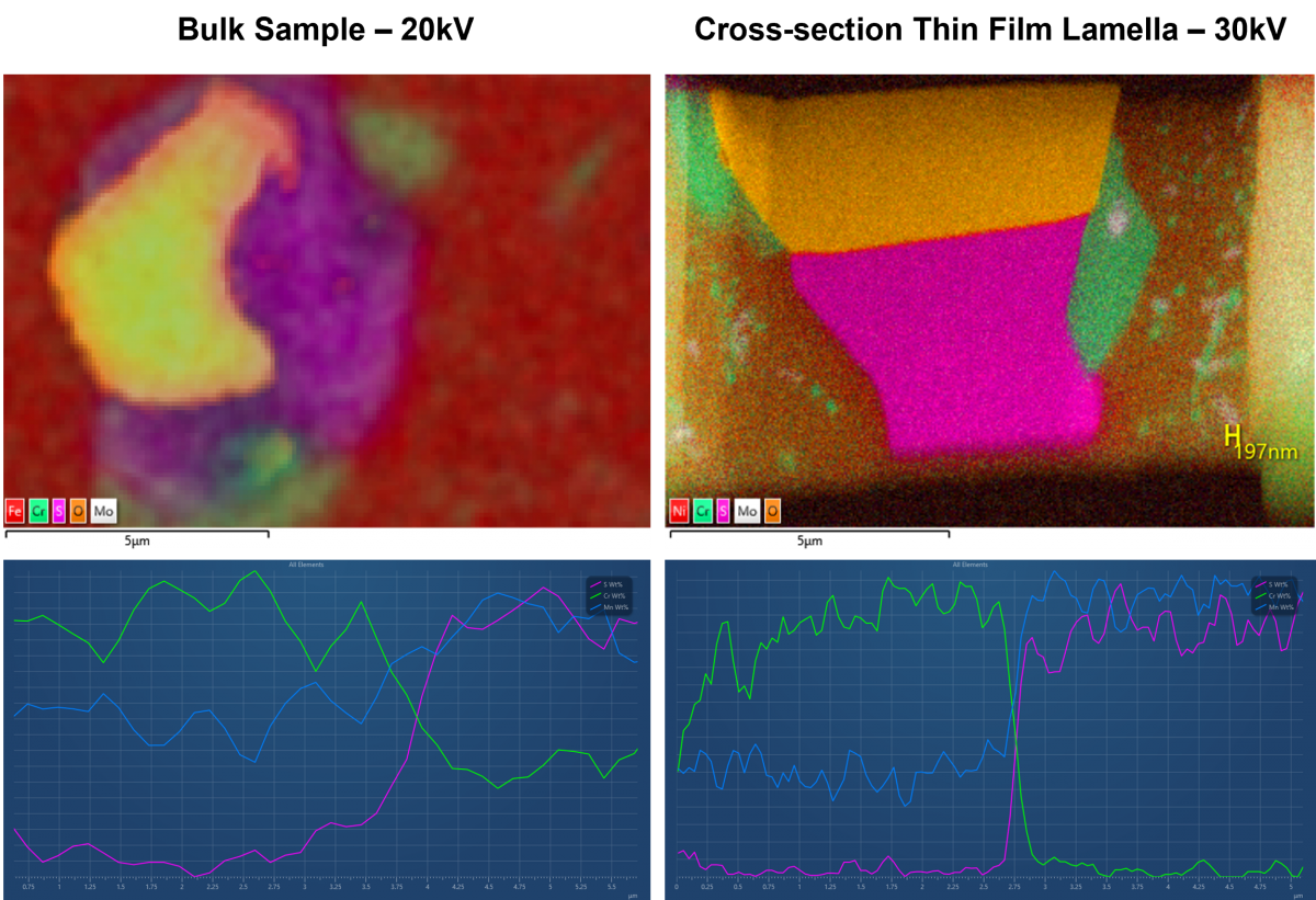
Figure 3 shows X-ray maps and linescans from typical multi-phase inclusions which contain a Mn-Cr spinel (orange), MnS (pink), Cr-rich sigma phase (green) and matrix (red-brown) from the bulk sample and a thin cross-section lamella. Close inspection of the two datasets shows the benefits of the improved spatial resolution in the lamella sample, the sharpness of grain boundaries, the uniformity of the composition within each phase (particularly around the grain boundaries), and most importantly, the detection of Cr- and Mo-rich nano-inclusions in the steel matrix. In the map from the bulk sample, only the largest Cr-rich inclusion in the top right is clearly visible. Inspecting linescans collected across the Spinel-MnS interface shows more clearly the difference in spatial resolution. In the bulk data, the change from one phase to the other is gradual over >750nm; in the lamella, it’s a clear step occurring over ~150 nm.

Figure 3. X-ray QuantMaps and QuantLinescans from the bulk and lamella samples
So, onto some actual quantitative analysis. For this blog, I’m focussing on the Mn-Cr spinel, MnS, and the matrix steel. Why? Because these phases have large enough areas to determine the composition using our highly reliable bulk analysis quantification, and the composition of these phases is the same throughout the sample. We can therefore be confident we know their composition. The Cr-rich sigma phase unfortunately has very variable Cr/Mo, and therefore I won’t consider it here.
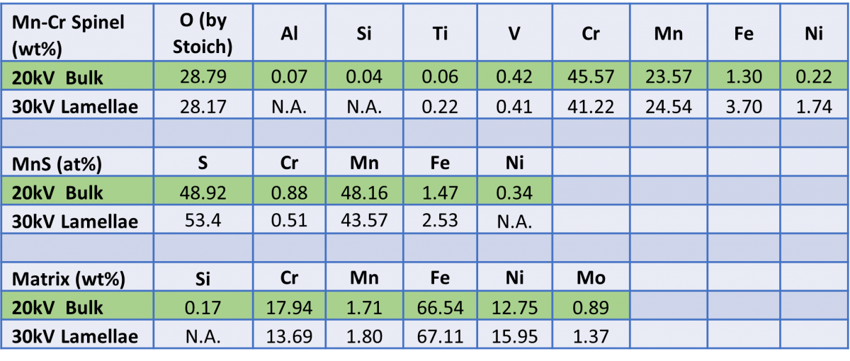
In Table 1, I compare the 20kV bulk composition (in green) with what I calculate by using the same bulk standardless quantification method on the phases in the lamella. This approach makes an incorrect assumption that the complete electron beam interaction is within the sample, the lamella is in fact semi-transparent to 30kV electrons and most are transmitted through the sample. Still, the results look encouraging and give at least an approximation of the sample composition. However, looking in detail, we have over-estimations in the heavier elements and under-estimations in the lighter ones.

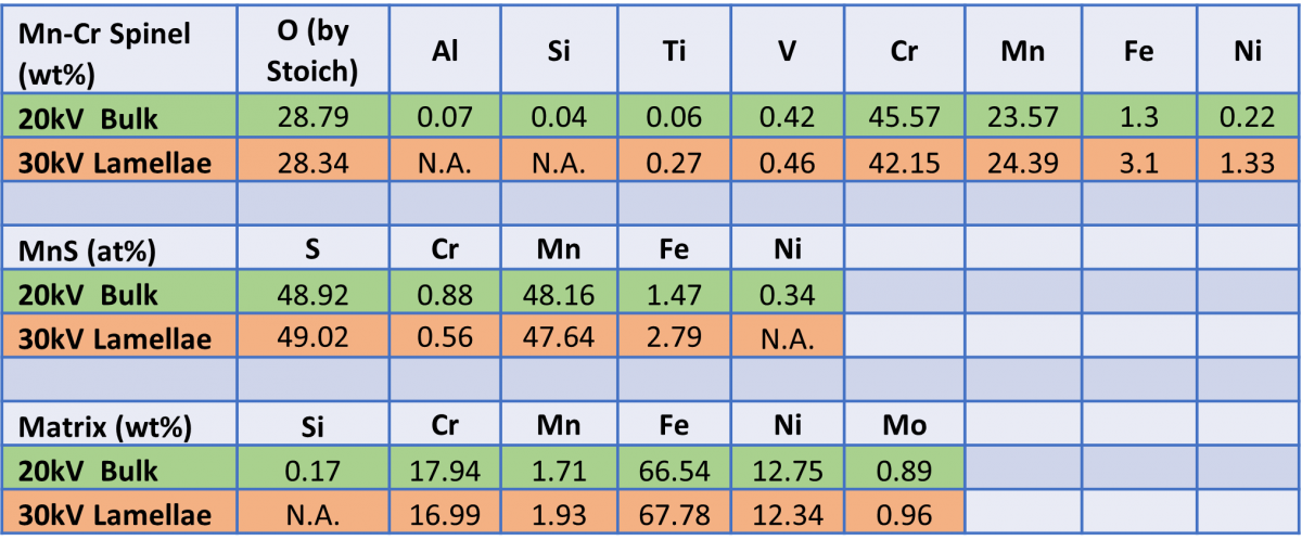
Can we do better? The answer is yes. The next approach is to use a thin film quantitative analysis method like that used in TEM at 120-300kV - the Cliff-Lorimer Method using k-factors. Does this work on a thin sample at 30kV? The TEM quantitative analysis software is available to analyse 30kV SEM-collected spectra in our AZtec software. Using this to re-calculate the results, we see a significant improvement. In Table 2, we are now comparing to the TEM quant (orange), and we see a much better agreement in composition for all three phases.

You might ask whether standardising (i.e. measuring standard materials using the same analytical conditions and not using the quant standardisations databases available in AZtec) would improve things further. We collected standards at 20kV and 30kV, but they make no significant improvement to the bulk results. This is fortunate, as the collection and calculation of k-factors is notoriously difficult, frustrating and time consuming, and may require you to make your own thin film standards if you can’t find any available commercially.
Can we do even better, and do we need to - as these results look pretty good? And a second obvious question is whether this will translate into useful analysis, such as the accurate compositional analysis of nano-structures that can’t be analysed at 20kV using a bulk sample. These are questions we shall tackle next time. For now, the take home message is 30kV analysis of thin film lamellae or other electron transparent samples offers not only improved spatial resolution for the characterisation of nano-structures in the SEM, but potentially also useful compositional analysis using a thin film (Cliff-Lorimer) quant analysis method, provided the quality of the standardless analysis is good.
You can learn about this in my earlier blog and webinars on how to check the accuracy of the compositions calculated by your system.
In the meantime, if you have questions about 30kV STEM-SEM quantitative analysis, or have tried it already and would like to share your experiences, then please contact us.


