18th August 2021 | Author: Anthony Hyde
Revolutionise your chemical imaging
“The ability to view a sample’s morphology and elemental distribution, simultaneously and continuously as you move around your sample”
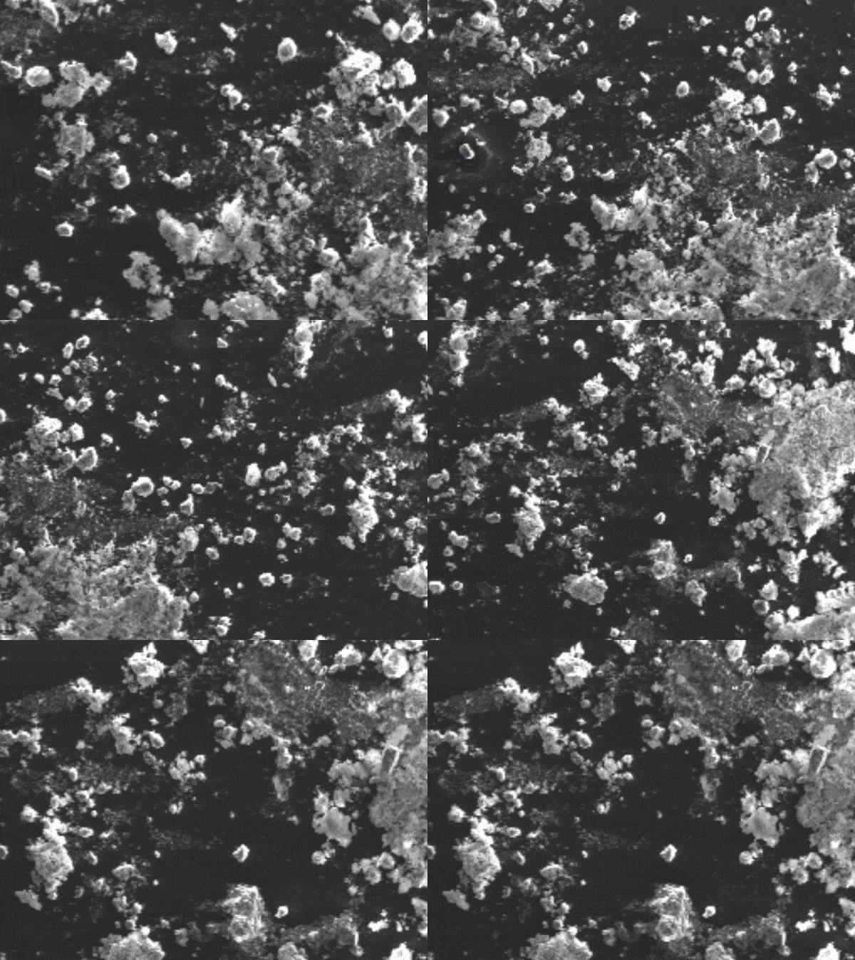
If you use a scanning electron microscope on a regular basis, then you will know that any sample investigation starts by viewing a fast-scanning live electron image. You will select a prominent feature of your sample to fine tune your focus and start moving around your sample to get a feel for its structure and topography.

Then, when you see something unusual or interesting, you’ll stop moving the stage to zoom in to the feature and acquire a slow scan electron image. After this you would probably switch over to your EDS system and repeat the image acquisition and acquire some spectra and perhaps X-ray maps to see what the elemental composition is and how these elements are distributed over the feature.
When you are satisfied you have gained enough information on the feature you will switch back to the live scanning electron image on the SEM and continue your visual inspection until you find another interesting feature.
All other EDS systems must employ this classic stop start workflow to their sample investigation, a live electron image is used to locate a feature of morphological interest, but they will have to stop the stage to acquire the x-ray maps. Once finished they will move on to the next area and the process will be repeated until they either:
- find what they were looking for
- have a representative view of their sample
This process is time consuming and sometimes inconclusive. The areas chosen for EDS analysis are chosen randomly, especially if the user is not familiar with the sample. As the user moves from one area to the next, they will miss any elemental distribution information while in transit.
Is there a better way?
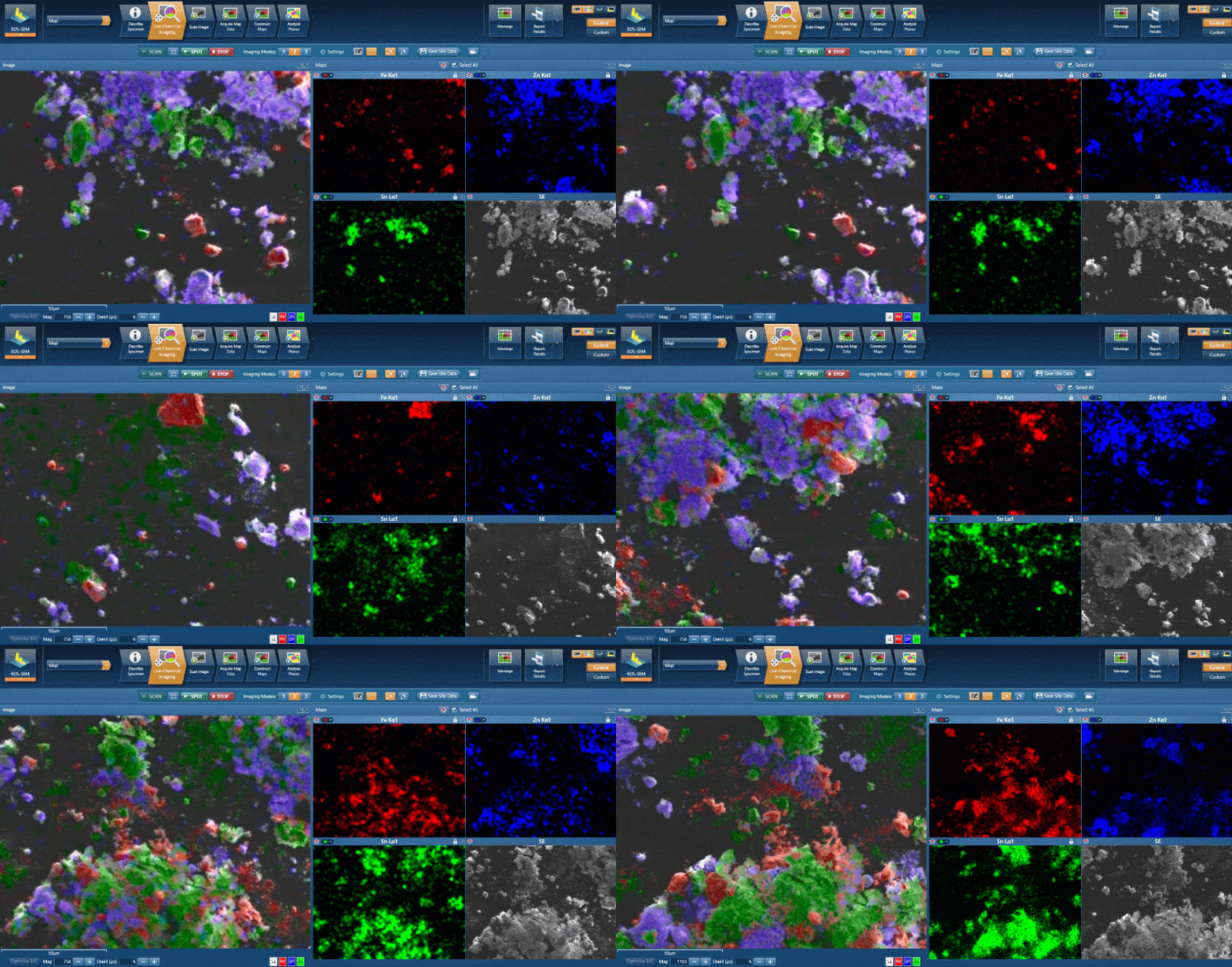
Imagine doing that same investigation, but with a live coloured image, and the colours in that image correspond to elements present in your sample.
So now, as you move around your sample you will not only be getting a feel for its structure and topography, but also its elemental composition and distribution.

This is what you can now do with AZtecLive Chemical Imaging. It makes sample investigation simple and powerful. There is no need to have advanced sample knowledge, no need to stop the SEM stage to perform EDS analysis and also means you won’t miss chemical information as you move from one area of your sample to the next.
Not having any prior sample knowledge of a sample can be a common occurrence in a contract lab. So, you need as much information and help from your SEM-EDS system as possible.
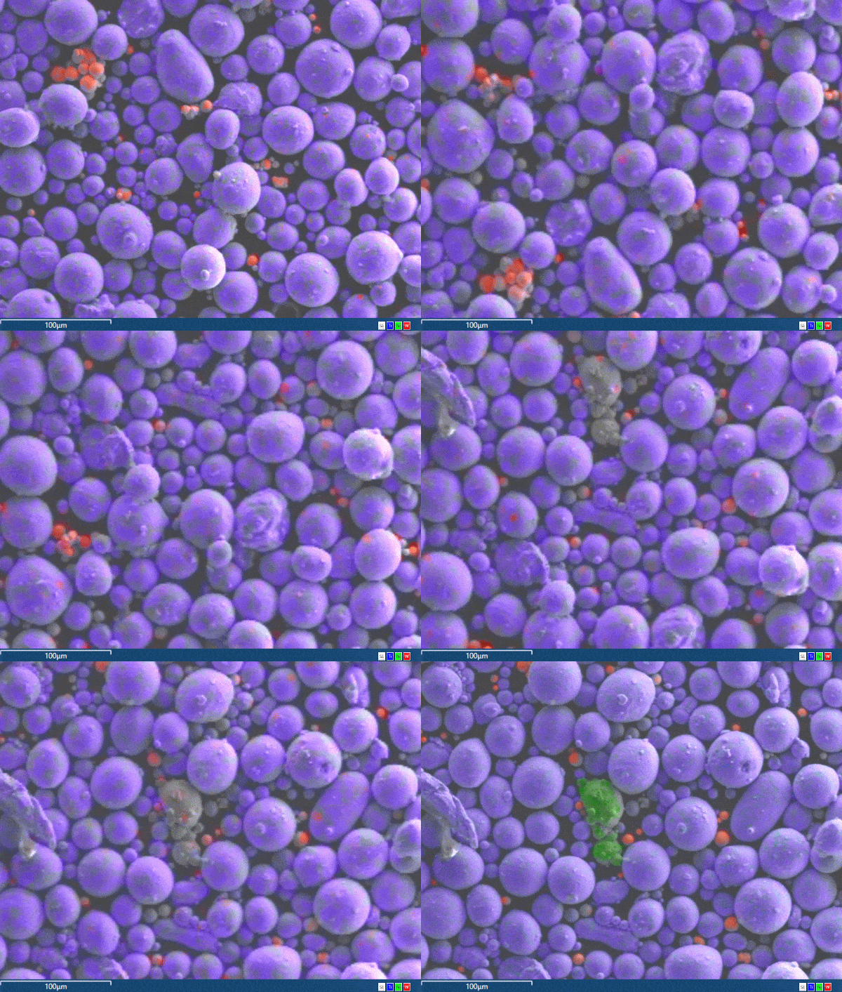
This example shows the live investigation of a 3D tungsten printer powder sample, where Live Chemical Imaging is used to quickly determine whether the sample is free from contamination.
Sure enough, as we start the analysis, the software automatically detects and adds the Titanium map (blue) and the Tungsten map (red) to the coloured image

Then as we move around the sample, Nickel contamination is detected, and the map (Green) is also automatically added to the colour image.
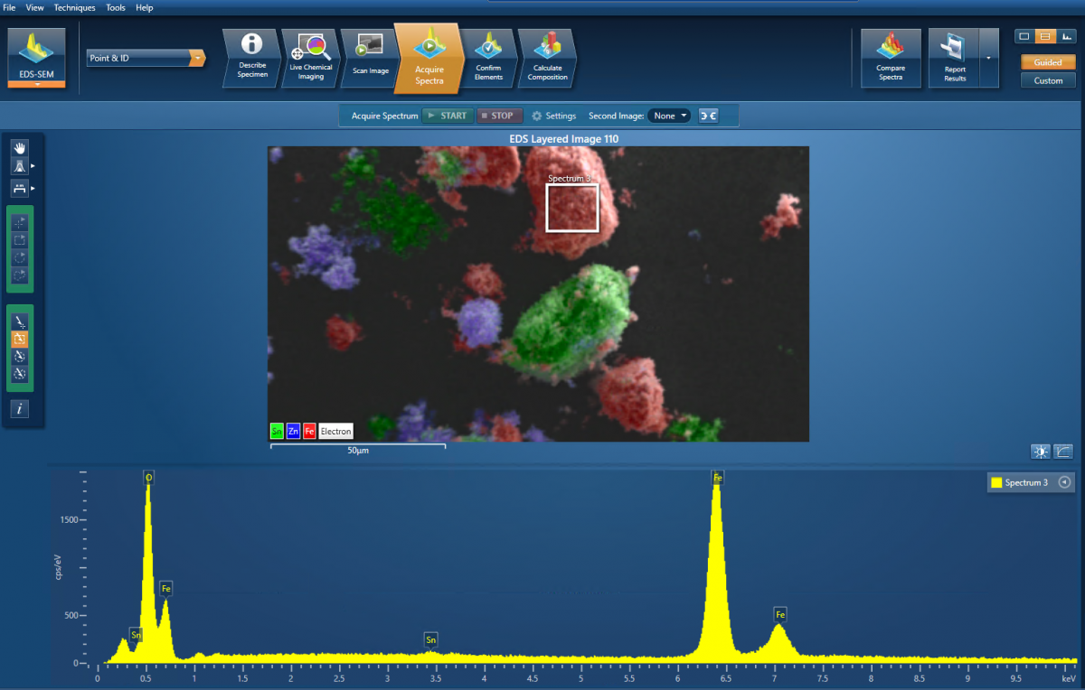
So, you can see that within seconds of turning the SEM beam on, you can get a comprehensive understanding of your sample’s morphology and chemistry. AZtecLive Chemical Imaging will give you continuous feedback as you move around your sample and anytime you pause, it will automatically go into integration mode and the sum spectrum will have time to detect any low concentrations of elements.
Learn more about the unique capabilities of AZtecLive Chemical Imaging by watching our recent launch webinar on demand.


