The performance of materials is dependent on their microstructure, composition, and processing history. With the development of modern electron microscopy analysis techniques, especially the great success in the commercialisation of large-area SDD EDS and CMOS-EBSD systems, the compositional and microstructural analysis of materials at the nanometre scale is no longer the prerogative of TEM. Recently, Wang et al. at Dongguan University of Technology China published their latest research in Scripta Materialia (click here
to view the full paper), with the help of Oxford Instruments Symmetry S2 fibre-optic-based CMOS-EBSD detector. In this work, nano precipitates in Ti22Nb alloys were studied by combining TKD and STEM-EDS.
Dr Hanxiao Wang, from Oxford Instruments China applications team, provided EM technical support for this work, where Symmetry S2 and Ultim Max EDS detectors were utilised to characterise the microstructure and element distribution of Ti22Nb alloys. Here, we extract STEM-EDS and TKD results from the publication which show the nature of needle-like precipitates in terms of their chemistry and crystallographic orientation relationship relative to the matrix.
Some Ti-Nb alloys have a unique linear zero-expansion property over a wide temperature range, which show great application prospects in high-value engineering structures that require high dimensional stability, such as aerospace, microelectronic devices, and optical instruments. Benefiting from the negative thermal expansion of the αʺiso
phase along its <010> crystallographic orientation, it is possible to obtain an alloy system (i.e., Ti22Nb) with zero thermal expansion by tailoring the volume fraction and preferred orientation of αʺiso. In order to achieve this it is very important to understand the precipitation mechanism of this phase and the use of EDS/EBSD as techniques for R&D of engineering materials is preferred because they are fast, reliable and easy to use.
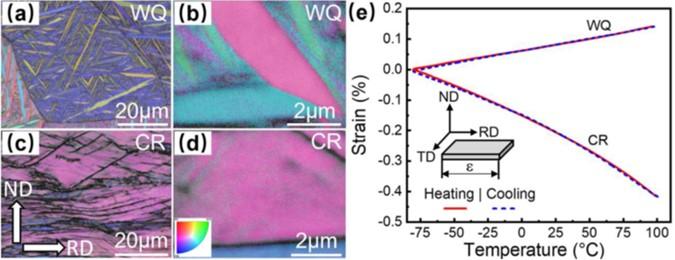
Figure 1 shows EBSD maps of water quenched (WQ) and cold rolled (CR) bulk samples, respectively, viewed along the sheet transverse direction. The WQ sample consists of fine laths of αʺ martensite with the equiaxed prior β grain structure still visible. Quenching stress resulted in local lattice distortion, which manifests itself as tiny fluctuations in IPF colour within individual grains. The CR sample has an even higher dislocation density, and the staggered deformation band morphology is an indicator of large plastic strain. The fibre-optic lens used in Symmetry S2 provides high sensitivity alongside high speed, making it a powerful tool for characterising such highly deformed samples.
Figure 1: EBSD band contrast (BC) maps overlaid with inverse pole figure (IPF) colouring of the microstructure of the Ti22Nb sheets in (a,b) water-quenched (WQ) and (c,d) cold-rolled (CR) conditions. (e) Single-cycle TMA measurements for the WQ and CR Ti22Nb sheets below the austenite start temperature. The inset in (e) shows the measuring direction is along the rolling direction (RD).
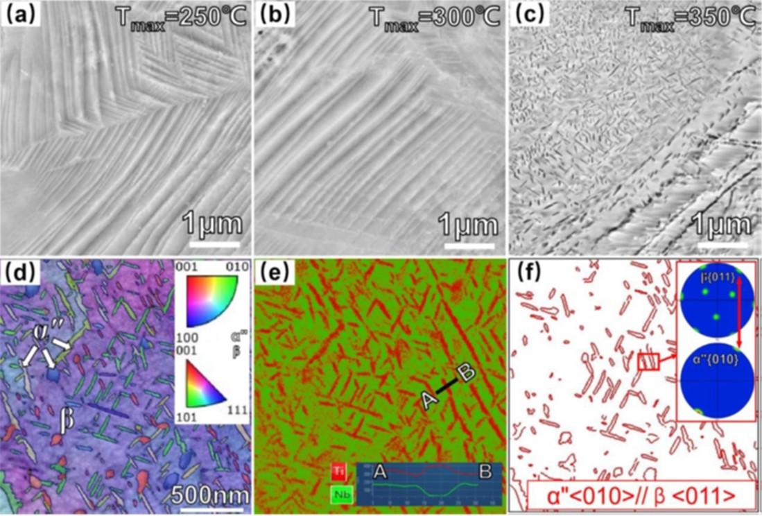
The thermal expansion coefficient of the CR samples decreased to zero after being kept at 350℃ for 10 min. To elucidate the underlying mechanism, Wang et al. investigated the effects of temperature gradient on the microstructure of Ti22Nb, as shown in Figure 2(a-c). The lamellar morphology of αʺ is still preserved at 250-300 °C despite the fact that the crystal structure has changed. A large number of needle-like nano precipitates became clearly visible after heating to 350 °C. In order to improve the spatial resolution of the analysis it was then decided to characterise these precipitates using the Transmission Kikuchi Diffraction (TKD) mode of Symmetry S2. The acceleration voltage and step size used were 30 kV and 5 nm, respectively.
Figure 2: SEM backscattered electron (BSE) image of Ti22Nb CR samples after heating to (a) 250 °C, (b) 300 °C and (c) 350 °C. (d) TKD band contrast (BC) overlaid with inverse pole figure (IPF) map inside a primary αʺmartensite lath in the same sample as in (c). (e) EDS map of Ti and Nb from the area shown in (d). The inset in (e) shows the element distribution along the line from A to B. (f) Highlighted β/ αʺphase boundaries that obey the orientation relationship <010> αʺ// <011> β. The insets in (f) show the pole figures of {011} β and {010}αʺ planes from the area indicated by the red rectangle.
The high spatial resolution TKD results show that the αʺ phase (with a minimum needle width of only 10 nm) is highly dispersed in the β matrix, and the two phases satisfy the <010> αʺ // <011>β relationship. Figure 2(e) is the STEM-EDS mapping simultaneously collected using a Ultim Max EDS detector. The element distribution map suggests that compared with the matrix, the needle-like precipitates are rich in titanium. By combining the crystallographic and chemical information, Wang et al. proposed that the second phase is consistent with the αʺiso reported in the literature and attributed the linear zero-expansion characteristic of the sample in Fig. 2(c) to αʺiso that derived from diffusive phase transformation.
With the help of neutron diffraction, EBSD, TKD and STEM-EDS, Wang et al. studied the microstructure of Ti22Nb alloys at a length scale ranging from micron to nanometre, thus providing a solid theoretical foundation for the design of linear zero-expansion titanium alloys. The high spatial resolution achieved the Symmetry S2 CMOS-EBSD and Ultim Max large-area EDS systems on SEM clearly played an important role in this work.