Minimise Curtaining
Curtaining is an artefact resulting when different materials, mill at different rates. It is most prevalent in samples where a hard, structured material (with a slow milling rate) is above or inside a soft material (fast milling rate) but also occurs when surface topography or voids (such as a crack) are present. On a cross-section, curtaining prevents good analysis, in TEM lamella preparation the thickness variations are catastrophic.

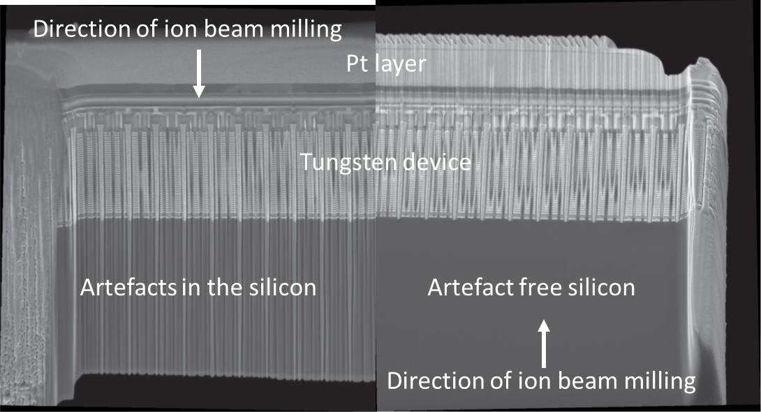
Left: image shows the detrimental effect curtaining has when milling a typical semiconductor device, consisting of metal (tungsten) features above a silicon matrix. In cross-section the curtaining produces artefacts in the silicon, the presence of these artefacts when attempting to thin the sample to electron transparency, will results in sample disintegration.
Right: how the device should look, milling artefacts are present, but only in the Pt layer, not the device.
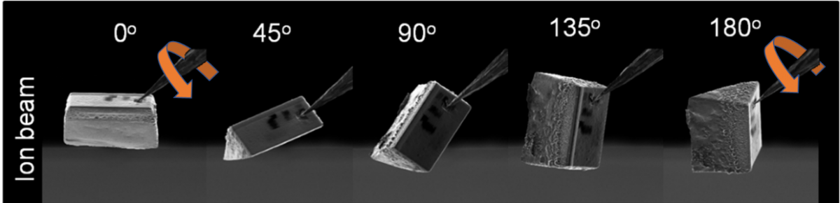
Curtaining can be minimised by optimising the milling direction. This typically means changing the orientation of the sample so that a uniform layer mills first, this will produce less curtaining. In this example, it requires inverting the sample so the silicon layer mills before the tungsten. During lamella lift-out, this can be achieved using an OmniProbe with the capability to rotate the sample in the chamber. However, rotating a lift-out sample on an OmniProbe tip by 180° will not invert the sample as all manipulators are mounted on at an angle relative to the sample. This challenge can be visualised (without needing a FIB) by rotating a post-it note (lamella) attached to a pencil (probe).

Sequence of ion beam images showing a sample rotation of 180° with an OmniProbe
To achieve sample inversion a combination of angles (probe and stage) can be calculated to create microscope specific recipes for vent free creation of a plan view sample (a sample rotated by 90°), combining this recipe with an OmniPivot (a TEM grid holder, which can pivot the grid without directly handling the grid) produces sample inversion. The result is a high-quality sample with minimised milling artefacts. The combination of an OmniProbe and OmniPivot means that almost any orientation sample can be created.
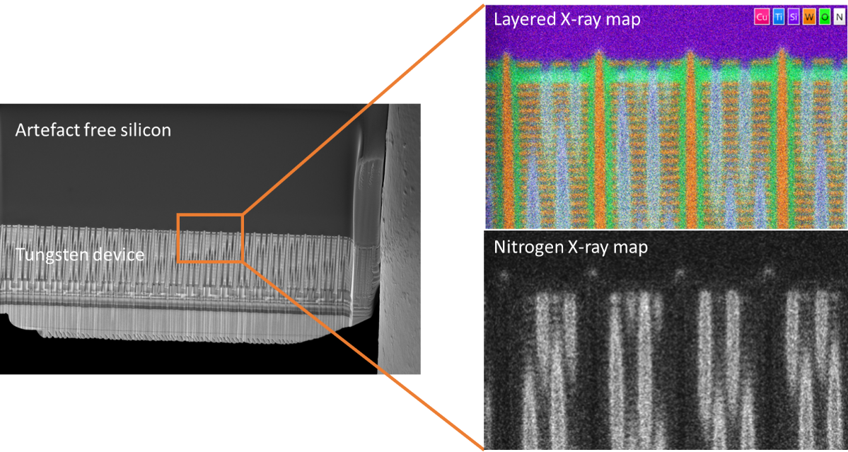
Same semiconductor device as above but inverted before milling. The silicon is artefact free, enabling the high-resolution EDS map acquired with an Extreme X-ray detector, to identify nitrogen at the bottom of the tungsten via’s.