Products
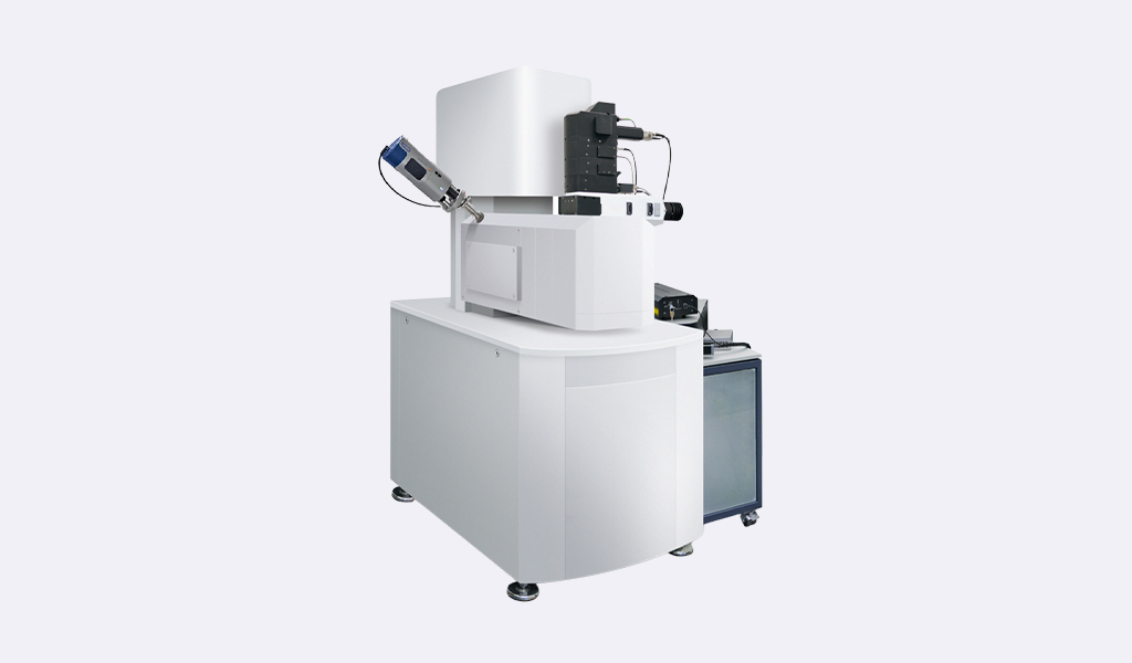
FIB-SEM
Nanomanipulators
OmniProbeOmniProbe CryoSoftware
AZtec3DAZtecFeatureAZtec LayerProbeTEM
Hardware
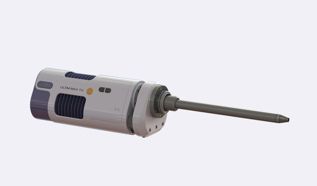
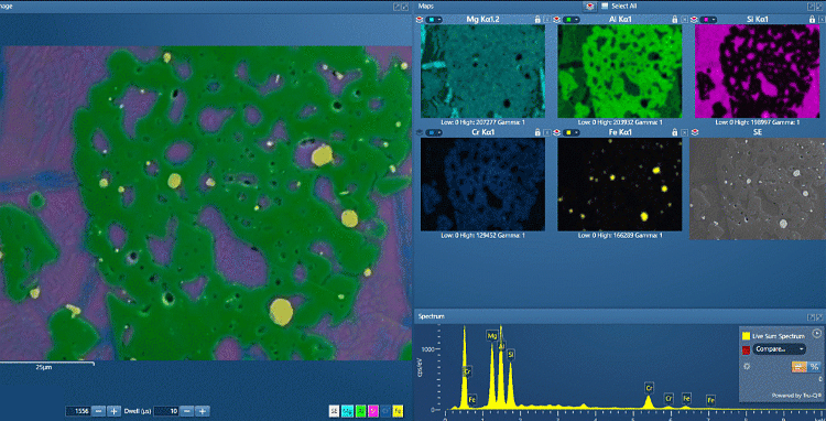
EDSUltim MaxXplore for TEMImaging
TEM CamerasSoftware
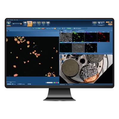
AZtecTEMRaman
RISE
Application Specific Software
Additive manufacturingAutomated mineralogyBattery materialsCorrelative microscopyFibre analysisGeological materialsGunshot residueHigh Temperature EDS analysisNon-metallic inclusionsParticle AnalysisPharma applicationsTechnical cleanlinessData Processing Software
AZtecFlexAZtecCrystalRelateSample Preparation
Ion Polisher


 Powered by Bioz