Part of the Oxford Instruments Group
Expand
AZtec Software

AZtecHKL

AZtecHKL is a powerful EBSD software platform that combines fast, accurate data acquisition and analysis with the flexibility required for advanced materials characterisation. Delivering real-time results, it maximises the performance of the Symmetry S3, the world’s most sensitive CMOS-based EBSD detector. The software also supports seamless simultaneous EBSD and EDS acquisition through AZtecSynergy and is optimised for nanoscale orientation mapping using Transmission Kikuchi Diffraction (TKD), making it ideal for both routine analysis and cutting-edge research applications.

Request Pricing

AZtecHKL is now enhanced with human expertise and artificial intelligence to make even the most powerful measurements routine.

AZtecHKL introduces powerful new tools that make advanced EBSD acquisition easier to set up, more consistent to run, and simpler to report. Designed for routine measurements as well as demanding applications, these features help users capture high-quality data, reduce setup complexity, and turn results into shareable insight with greater confidence.

Tailored Workflow

  • A licensed option that brings Oxford Instruments’ EBSD expertise directly into AZtecHKL, optimising system configuration for recurring measurement requirements.
  • Fine tunes acquisition parameters for specific systems and sample types to maximise performance and consistency.
  • Guides users through complex experiments with a custom step-by-step navigator, enabling faster setup and supporting robust standard operating procedures.

EBSD Shadow Masking

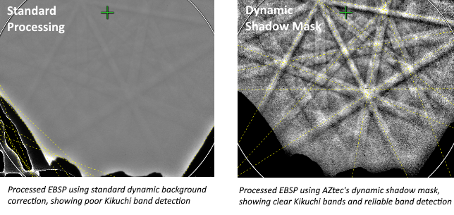
  • Uses artificial intelligence to suppress dynamic EBSP shadows that can interfere with EBSD band detection.
  • Reduces the impact of shadows caused by rough or complex sample geometries, helping reveal otherwise obscured details.
  • Particularly valuable for challenging applications such as fracture surface investigation, failure analysis, and focused ion beam trench analysis.

Batch Export

  • Enables efficient export of large EBSD datasets, including AutoPhaseMap outputs.
  • Supports saving data in preferred file formats and sizes for downstream use.
  • Streamlines post-acquisition data handling and transfer into established analysis, archiving, and reporting workflows.

HTML Project Report

  • Automatically generates a complete report from an EBSD session while maintaining the project structure.
  • Simplifies review, documentation, and sharing of results.
  • Provides a consistent record of measurement setup, acquisition, and analysis to support clear communication of findings.
Unmatched in breadth and accuracy, AZtecHKL is a must for anyone serious about EBSD analysis...

AZtec couples Oxford Instruments’ understanding of real customer needs for routine EBSD analysis, with the flexibility and power required for applications that push the frontiers of EBSD.

Developed by the market leader with global customer support and over 40 years experience in nanoanalysis, AZtec meets the ever more challenging requirements of analysis at the nanoscale.

Fast and powerful

  • Unleash the latest generation of CMOS EBSD detectors for high-speed and high-sensitivity data acquisition
  • Acquire, process and display high-speed data in real-time
  • Interact with your data during acquisition using 64-bit processing power and multitasking software

Easy to use

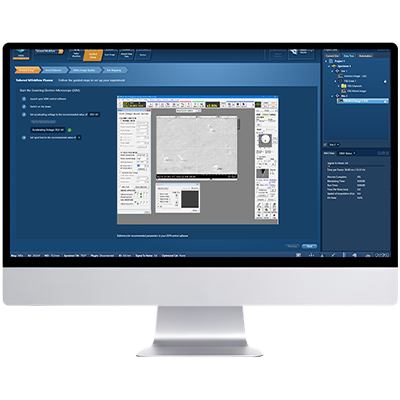
  • A guided workflow for system set-up and data acquisition ensures that everyone gets the right results every time
  • Intelligent tools, such as automatic background correction, ensure accurate results on all samples
  • Dedicated TKD analysis navigator facilitates excellent data acquisition from nanostructured materials
  • Unique Optimise Experiment step to assist users in finding the best settings for every sample and analysis type

Flexible

  • Experts can adjust settings to solve difficult applications
  • Optimise data post-acquisition using powerful re-analysis tools
  • Present data and results in customisable reports

Innovative

  • Unique Tru-I® algorithms achieve the highest number of accurately indexed EBSPs
  • Simultaneous EBSD and EDS analysis, including using EDS data to differentiate similar crystal structures
  • Patented refined accuracy indexing delivers an outstanding angular resolution as low as 0.01˚
  • Powerful tools included as standard, e.g. dynamic shadow-masking for optimal data quality from rough samples and in 3D-EBSD analyses

Downloads

App note: Determining the metamorphic history of rocks using combined EBSD and EDS

Reconstructing the metamorphic evolution of rocks often depends on the identification of key minerals that are only stable at specific temperatures and pressures. Combined EBSD and EDS analyses enable more rigorous phase identification than conventional techniques, with the added benefit of providing insights into a rock’s deformation and chemical history.
Download
EBSD Explained

EBSD Explained is a 24 page tutorial that not only gives newcomers a solid foundation in the underlining science of the subject, but also shows how the theory is applied in practice to get reliable and accurate EBSD results.

Download
Symmetry S3

Symmetry S3 is a 3rd generation detector based on the advanced CMOS technology and unique design features that have made Symmetry the market’s leading EBSD detector.

Download

Video

The Latest Developments in EBSD Software

We discuss the developments to our EBSD acquisition and data processing including a new guided workflow in AZtecHKL to assist with setting up and running Transmission Kikuchi Diffraction experiments and a versatile new Parent Grain Analysis viewing mode within AZtecCrystal that enables rapid reconstruction of parent microstructures.

Approx View time: 7 minutes

Additional Features of AZtecHKL

AZtec Tru-I, the EBSD indexing engine, ensures that users collect the best quality patterns and can solve them accurately, reliably and automatically. Pattern collection and solving are performed in real-time.

Collect the high-quality patterns which are essential to obtaining accurate EBSD data.
  • AZtec has an optimised system design, for the collection of excellent patterns, even at high speeds or high binning
    • The signal strength and noise are quantified and can be used as a measure of pattern quality

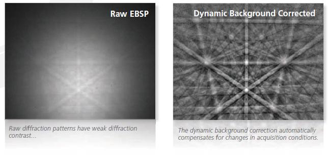
Dynamic background correction enables pattern by pattern contrast optimisation.
  • Excellent quality patterns can be achieved from all materials
    • includes multiphase materials, where the phases can have significantly different atomic numbers
  • Dynamic background correction automatically masks screen imperfections
  • Dynamic shadow masking ensures high quality patterns and results, even when parts of the screen are shadowed (as in some 3D analyses)
Shadow_Mask
Intelligent band detection

AZtec implements an intelligent band detection routine that determines which of the detected bands should be used in the indexing.

  • Intelligent band detection uses both the average intensity of the band and its position in the area of interest
  • Improves the percentage of correctly indexed points, especially for materials exhibiting indistinct bands or where pattern quality is low

Magnetic Field Correction solves distorted patterns

In some applications, high magnetic fields from the SEM lenses distort the electron backscattered diffraction patterns. This distortion curves the Kikuchi bands and shifts the pattern centre but can be corrected automatically using AZtec.

  • The correction straightens the bands and corrects the pattern centre so patterns can be correctly solved
  • A dipole correction described in Oxford Instruments’ US patent 7442930B2 is applied
Class Indexing

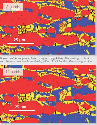
The EBSD indexing routine is critical in achieving accurate results - AZtec uses a new method, Class Indexing.

  • This method is robust and the correct solution can be achieved even if one or more detected band is not included in the list of reference reflectors
  • The system is less sensitive to the operator selecting the number of bands and reflectors
Distinguish similar crystal structures

AZtec correctly identifies phases with similar crystal structures by comparing bandwidth.

Refined Accuracy Algorithm

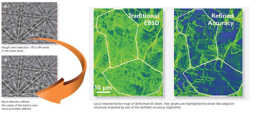
A new and innovative ‘Refined Accuracy Algorithm*’extends traditional EBSD analysis to deliver unrivalled accuracy and level of detail...

  • Refines the position of the Kikuchi bands after indexing so the most accurate orientation measurements are achieved
  • Overcomes the well-documented limitations of the Hough transform
  • The Ni patterns (below) illustrate the optimisation benefits:
    • Pattern A shows the initial band detection based on Hough
    • Pattern B shows the band position after refinement by the new method

AZtec Refined Accuracy delivers:

  • Class-leading orientation measurement accuracy ...in real-time
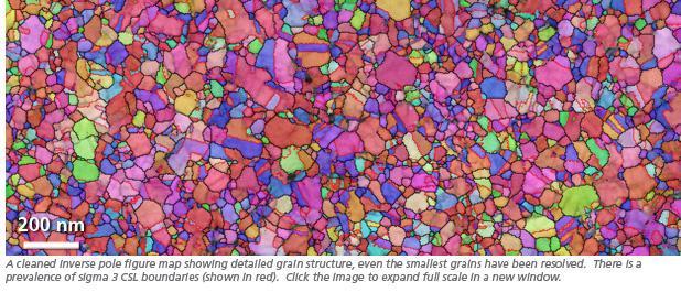
    • enhances boundary characterisation
    • identifies subtle subgrain microstructures
    • optimises the fit between the acquired pattern and solution

AZtecHKL contains many intelligent EBSD Acquisition Tools that make data acquisition faster, easier...better

AutoCal
Change acquisition conditions and still collect quality EBSD patterns at the click of a button

  • Collect accurate data routinely under a full range of working distance and detector insertion distance – without recalibrating
  • AutoCal is a sophisticated geometric correction which works seamlessly and automatically to calculate calibration parameters based upon changes in geometry
  • Compensates for changes to the projection parameters resulting from beam movement at low magnification
  • The system is quick and easy to set up, whatever the user experience level

AZtec corrects for changes in acquisition conditions automatically and in real-time

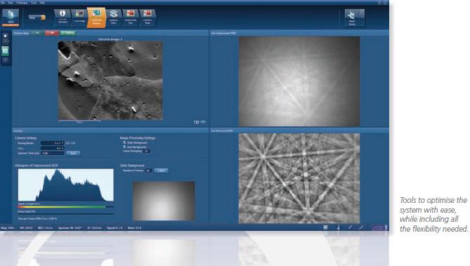
Optimising the system for data acquisition is easier and more automated than ever before

  • Automatic detector exposure
  • Intelligent dynamic background
  • Detector control from within the user interface
  • Change SEM conditions – kV, probe current, magnification, or stage tilt – without recalibrating,
    • and still, collect an optimised EBSP which is correctly solved

AutoLock

  • AutoLock is an integrated drift correction tool that corrects EBSD and EDS data simultaneously, resulting in the most accurate maps.
  • A unique blend of predictive and reactive drift correction routines
  • Corrects drift on tilted and untilted samples
  • Essential for high magnification nanoscale EBSD

Image Registration

All AZtec acquired images can be used for specimen navigation and relocation at a later date - even on a different microscope.

  • AZtec takes control of the microscope stage and seamlessly relocates to points of interest
  • During a session, any acquired image or map is automatically registered, enabling easy relocation to previously analysed areas#
  • Any image can be used for navigation i.e. an EBSD map can be used to navigate to an area of interest
  • Manually registering images enables specific areas of a specimen to be further investigated at a later date, even on another microscope

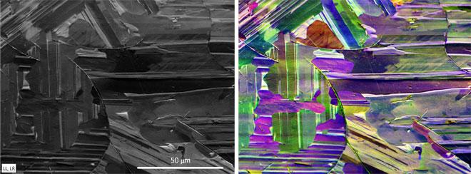
Microstructure Imaging using Forescatter diodes (FSD) highlights regions of interest for further investigation. AZtec, coupled with any of our CMOS-based EBSD detectors, is a powerful solution for all EBSD applications.

The CMOS detectors can incorporate up to 5 forescatter detector diodes

  • AZtec enables independent image acquisition from each diode
  • Flexibility to customise and mix any combination of these images
  • Automatic colour FSD highlights details that may be missed by greyscale imaging alone

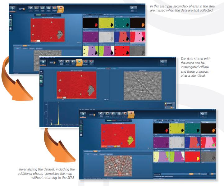
Optimise settings and re-analyse without needing to re-acquire data. With AZtecHKL users can process both post-acquisition and offline.

AZtecHKL re-analysis is completely flexible:

  • Optimise solver settings, or add additional phases, and re-analyse the data offline
  • It is not necessary to know all the phases in the sample before acquiring data

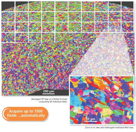
AZtec Large Area Mapping enables the unattended collection of high-resolution data (images with simultaneous EBSD and EDS maps) from large specimen areas.

  • A setup wizard guides users through the process, making Large Area Map acquisition routine
  • Designed for tilted EBSD geometry to ensure that sample focus is maintained during acquisition
  • Automatic image alignment during acquisition ensures a seamless LAM dataset both before and after montaging
  • Acquire up to 1500 fields at 8K image resolution and 4K EBSD map resolution to create an image data set of 96 billion pixels and an EBSD dataset of 24 billion pixels
  • Interactive both during and after acquisition: view all the data in the large image and zoom into the fine detail
  • A single montaged data set (up to 64 Million datapoints in size) can be interrogated in AZtec as a standard Site of Interest to extract:
    • X-ray maps, EDS layer maps, Autophase maps and spectra
    • IPF, Euler and phase maps, and individual EBSPs


TKD (Transmission Kikuchi Diffraction, sometimes referred to as t-EBSD), used for the collection of EBSD data in transmission mode in the SEM, is increasingly applied for materials characterisation at the nanoscale.

Despite significant technological developments in recent years, the conventional EBSD technique is still limited by the pattern source volume to resolutions in the order of 25-100 nm. This is insufficient to measure accurately truly nanostructured materials (with mean grain sizes below 100 nm).

A new approach to SEM-based diffraction has emerged. This uses an electron-transparent sample coupled with conventional EBSD hardware and software. This technique referred to as transmission EBSD (t-EBSD: Keller and Geiss, 2012) or SEM Transmission Kikuchi Diffraction (TKD: Trimby, 2012) has been proven to enable spatial resolutions better than 10nm.

TKD in AZtec

AZtecHKL includes a dedicated TKD navigator that, coupled with the exceptional sensitivity of our CMOS detector range, always delivers high quality TKD results. There are a number of unique TKD-focused innovations, enabling an instantaneous switch from conventional EBSD analyses to TKD:

  • TKD-specific sample geometries and set-up
  • Automated darkfield and oriented darkfield imaging using forescatter detectors
  • Optimised band detection, using higher resolution Hough-peak analysis to ensure perfect band detection in highly distorted TKD patterns
  • Software-controlled detector elevation (Symmetry S3 detector) ensuring perfect TKD patterns every time
TKD advantages
  • Spatial resolution better than 10 nm
  • Ideal for the routine characterisation of nanostructured material
  • EBSD analysis of highly deformed samples

Related Products

Symmetry S3

Symmetry S3

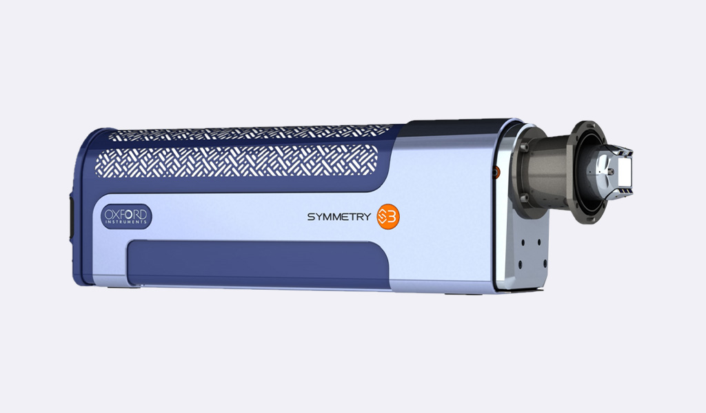
The Symmetry S3 is the only genuine all-in-one EBSD detector on the market, and is based on the revolutionary Symmetry detector, the world’s first EBSD detector to utilise advanced CMOS technology.

C-Swift+

C-Swift+

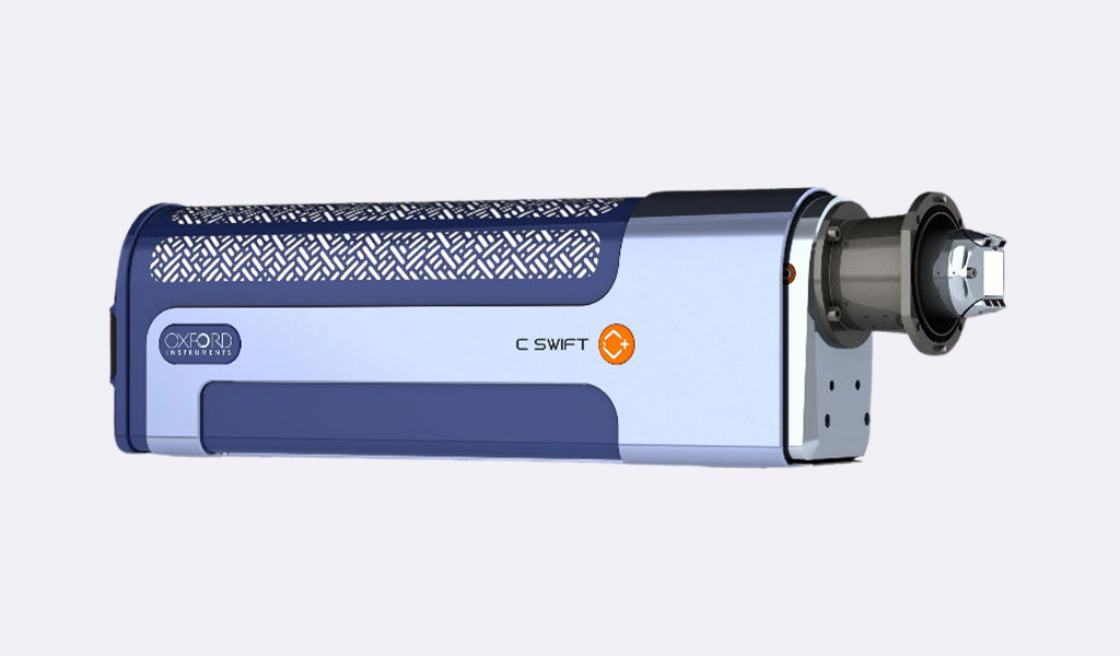
The C-Swift+ is a high-speed and versatile entry-level EBSD detector designed for routine materials analysis and high throughput sample characterisation, offering an ideal balance of performance, ease of use, and value.

C-Nano+

C-Nano+

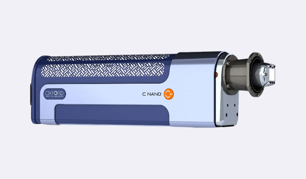
The C-Nano+ is suited to characterising all types of samples, but its high pixel resolution makes it ideal for detailed strain analyses as well as for routine work on complex and challenging materials.